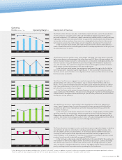
Pentax 2009 Annual Report Download - page 14
Download and view the complete annual report
Please find page 14 of the 2009 Pentax annual report below. You can navigate through the pages in the report by either clicking on the pages listed below, or by using the keyword search tool below to find specific information within the annual report.-
 1
1 -
2
-
3
-
 4
4 -
 5
5 -
 6
6 -
 7
7 -
 8
8 -
 9
9 -
 10
10 -
 11
11 -
 12
12 -
 13
13 -
 14
14 -
 15
15 -
 16
16 -
 17
17 -
 18
18 -
 19
19 -
 20
20 -
 21
21 -
 22
22 -
 23
23 -
 24
24 -
25
-
26
-
27
-
28
-
29
-
30
-
31
-
32
-
33
-
34
-
35
-
36
-
37
-
38
-
39
-
40
-
41
-
42
-
43
-
44
-
45
-
46
-
47
-
48
-
49
-
50
-
51
-
52
-
53
-
54
-
55
-
56
-
57
-
58
-
59
-
60
-
61
-
62
-
63
-
64
-
65
-
66
-
67
-
68
-
69
-
70
-
71
-
72
-
73
-
74
-
75
-
76
-
77
-
78
-
79
-
80
-
81
-
82
-
83
-
84
-
85
-
86
-
87
-
88
-
89
-
90
-
91
-
92
-
93
-
94
 |
 |

MASK BLANKS FOR
SEMICONDUCTOR PRODUCTION
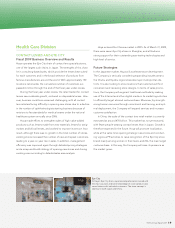
Fiscal 2009 Business Overview and Results
Hoya produces photomasks, which are the master plates used to
transfer the semiconductor circuit patterns to silicon wafers, and the
mask blanks that form the substrate for the photomasks. The Com-
pany supplies these products to semiconductor manufacturers in
Japan and overseas and boasts an overwhelming share of the global
market for mask blanks, particularly high precision mask blanks.
In the fiscal year under review, business in the semiconductor
industry was robust during the first half. Against the backdrop of an
economic slowdown that began in the second quarter, however, the
second half witnessed large-scale reductions in production and
curtailment of product development budgets and capital invest-
ments in the industry. Amid these market movements, sales of mask
blanks fell in the second half because of the sharp drop in demand
and pressure on prices, producing an overall decline in sales year
on year. Even high precision products, such as the phase-shift mask
blanks*1 that had driven earnings growth in the past, faced a dif-
ficult business environment.
Future Strategies
Despite steady progress in cutting edge semiconductor develop-
ment, mass production of the devices utilizing these chips have
slowed the pace at which the industry shifts to the next generation
of semiconductors. Consequently, a clear gap has opened up
between technology progress and market needs. Furthermore, with
the steadily worsening business climate surrounding the semicon-
ductor industry, individual companies are limiting their investments
in chip development and focusing their efforts on building cost-
conscious, efficient production systems.
In recognition of these market needs, Hoya’s strategy has been
seeking other ways of increasing the degree of satisfaction of its
customers besides its miniaturization-oriented product develop-
ment by providing customers with added value. Its efforts have
included material development to further heighten the durability
of its products.
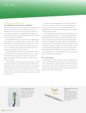
PHOTOMASKS FOR
SEMICONDUCTOR PRODUCTION
Fiscal 2009 Business Overview and Results
A photomask is a mask blank onto which a pattern has been drawn
with an electron beam or laser writing device. Hoya has developed
a highly competitive business model in the photomask market,
strongly developing the business by specializing in cutting edge
technology development and by taking advantage of in-house
mask blank operations to differentiate itself from competitors in
terms of its material processes.
In the fiscal year under review, Hoya put effort into providing
high-quality, cutting edge photomasks. Although there were some
successes with the introduction of new types of photoresist films
and mask blank materials compatible with cutting edge manufac-
turing processes for semiconductors, such as immersion lithogra-
phy, adverse business conditions such as stagnation in the
semiconductor market, a slump in demand for photomasks and
downward pressure on prices resulted in lower sales year on year.
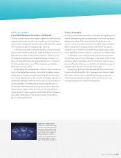
Electro-Optics Division
Illustration of circuit pattern
transfer using a lithographic
exposure process during semi-
conductor production
Mask blanks
From the left: a glass sub-
strate, a phase-shift halftone
mask blank, a homogenous
metallic film coated layer and
a completed blank with photo-
resist coating.
Light source
Condenser lens
Reduced projection
exposure lens unit
Photomask
Wafer
(semiconductor chip)
Hoya contributes to an abundant and prosperous future through advanced technology supporting progress in the functions
and value-added content of digital products, such as personal computers and large flat panel LCD televisions.
INFORMATION TECHNOLOGY
12 HOYA Annual Report 2009