Pentax 2008 Annual Report Download - page 28
Download and view the complete annual report
Please find page 28 of the 2008 Pentax annual report below. You can navigate through the pages in the report by either clicking on the pages listed below, or by using the keyword search tool below to find specific information within the annual report.-
 1
1 -
2
-
3
-
4
-
5
-
6
-
7
-
8
-
9
-
10
-
11
-
12
-
13
-
14
-
15
-
16
-
17
-
 18
18 -
 19
19 -
 20
20 -
 21
21 -
 22
22 -
 23
23 -
 24
24 -
 25
25 -
 26
26 -
 27
27 -
 28
28 -
 29
29 -
 30
30 -
 31
31 -
 32
32 -
 33
33 -
 34
34 -
 35
35 -
 36
36 -
 37
37 -
 38
38 -
39
-
40
-
41
-
42
-
43
-
44
-
45
-
46
-
47
-
48
-
49
-
50
-
51
-
52
-
53
-
54
-
55
-
56
-
57
-
58
-
59
-
60
-
61
-
62
-
63
-
64
-
65
-
66
-
67
-
68
-
69
-
70
-
71
-
72
-
73
-
74
-
75
-
76
-
77
-
78
-
79
-
80
-
81
-
82
-
83
-
84
-
85
-
86
-
87
-
88
-
89
-
90
-
91
-
92
 |
 |

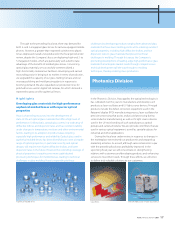
R&D and Intellectual
Property Activities
The Hoya Group pursues the twin objectives of achieving
sustainable growth and increasing corporate value. The Group
devotes considerable effort to strategic business planning and
technology R&D that focus on the long term.
The saying, be “a big fish in a small pond,” is one straight-
forward way of expressing Hoya’s business strategy. The “big fish”
refers to Hoya’s top market share, and the “small pond” refers to
the niche markets in which Hoya is active. Those markets may not
be immense, but Hoya maintains its position as an industry-
leading company in every one of them. The idiom about being a
big fish in a small pond succinctly expresses Hoya’s business
strategy for R&D, as well. Hoya strives to develop technologies and
cultivate new businesses that will, in the future, make Hoya a big
fish in a small pond.
The Company’s business integration with Pentax in the fiscal year
under review should result in advances in the opto-electronics
technologies Pentax has cultivated in endoscopes, digital cameras
and other precision equipment, as well as deeper synergies with
Hoya in the field of optics. The business integration with Pentax
should also result in advances in technological development in the
new growth field of endoscopes and other medical devices. This field
has grown in recent years, spurred by ongoing advances in medical
care. As medical practices are expected to become more advanced
and needs to diversify, we will apply our technical superiority to this
field of business, exercising our potential as a big fish in a small pond.
The Hoya Group delegates a lot of authority and responsibility to
its business divisions. In research and development, each division
follows its own next-generation R&D as a natural extension of its
current activities. The R&D Center at Hoya’s Global Headquarters
operates with a longer-term viewpoint and is engaged in research
that will lead to the development of the technologies that will
follow next-generation technologies, as well as research in new fields.
Here, we look at Hoya’s principal research themes. We also
introduce new fields of development that have emerged through
the integration with Pentax.
Developing 3C-SiC cubic monocrystal silicon carbide as a
prospective energy-efficient semiconductor
Preventing global warming is a worldwide concern, with energy
conservation measures being actively implemented in a broad
range of regions and industries. In view of this trend, Hoya is
promoting the development of 3C-SiC cubic monocrystal silicon
carbide semiconductor devices that are expected to offer superior
energy efficiency.
In comparison with ordinary silicon-based devices, 3C-SiC
devices are characterized by lower power loss and can operate at
high temperatures. When used in hybrid and fuel cell powered
vehicles, apart from the low energy consumption, they should
have lower production costs due to
their smaller size and the lower
weight of cooling systems. With the
goal of a practical application in
2010, Hoya is developing
technologies for the production of
large-diameter 3C-SiC wafers.
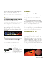
Fabricating nanoimprint molds, a technology regarded as a
gateway to the “terabyte*1 age”
The market continues to demand smaller and denser semi-
conductors to boost performance and reduce manufacturing
costs. However, the lithography processes used to transfer circuit
patterns onto semiconductors present substantial challenges in
curtailing production equipment and component costs, which are
ballooning as semiconductors are miniaturized. Nanoimprint
technologies are being spotlighted as a possible solution.
Nanoimprint technology applies printing techniques to create
an ultra-fine mold from which the circuit pattern is transferred by
stamping—one of the cheapest means of producing large
numbers of ultra-fine patterns.
Nanoimprint technology enables
the formation of patterns with line
widths of as small as a dozen
nanometers and is attracting
attention as an effective
technology for discrete track
recording media, which is regarded
as the next generation of recording
media for hard disk drives. This
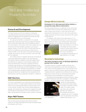
Research and Development
R&D Structure
Major R&D Themes
Energy-efficient materials
Nanoimprint technology
3C-SiC
1 nanoimprint template (mold) for
32 nm node production
26