Pentax 2008 Annual Report Download - page 15
Download and view the complete annual report
Please find page 15 of the 2008 Pentax annual report below. You can navigate through the pages in the report by either clicking on the pages listed below, or by using the keyword search tool below to find specific information within the annual report.-
 1
1 -
2
-
3
-
4
-
 5
5 -
 6
6 -
 7
7 -
 8
8 -
 9
9 -
 10
10 -
 11
11 -
 12
12 -
 13
13 -
 14
14 -
 15
15 -
 16
16 -
 17
17 -
 18
18 -
 19
19 -
 20
20 -
 21
21 -
 22
22 -
 23
23 -
 24
24 -
 25
25 -
26
-
27
-
28
-
29
-
30
-
31
-
32
-
33
-
34
-
35
-
36
-
37
-
38
-
39
-
40
-
41
-
42
-
43
-
44
-
45
-
46
-
47
-
48
-
49
-
50
-
51
-
52
-
53
-
54
-
55
-
56
-
57
-
58
-
59
-
60
-
61
-
62
-
63
-
64
-
65
-
66
-
67
-
68
-
69
-
70
-
71
-
72
-
73
-
74
-
75
-
76
-
77
-
78
-
79
-
80
-
81
-
82
-
83
-
84
-
85
-
86
-
87
-
88
-
89
-
90
-
91
-
92
 |
 |

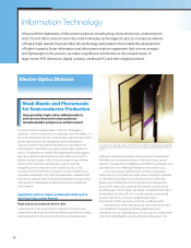
semiconductor industry, chip manufacturers are regarding
manufacturing cost reduction as a key issue even as they
accelerate development in leading-edge applications, resulting in
more complex, high-level needs from photomask manufacturers
than ever before. In line with this shift, the Company maintains a
development system intimately coordinated with its customers, at
times even getting involved in customers’ circuit design and
product development activities. Such coordination allows us to
offer not only cutting-edge technology development, but also
truly valuable solutions, such as products that increase yields on
customers’ production lines.
* One nanometer equals one billionth of a meter.
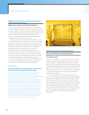
The argon fluoride excimer laser with a wavelength of 193 nm is
currently the predominant light source used for lithographic
exposure onto semiconductor wafers. The circuit patterns that the
ArF excimer laser can draw were considered to be limited to a line
width of 65 or 45 nm. However, as of 2008, advances in production
techniques have brought 22 nm pattern formation into view. On
the other hand, the strongest candidate for the next generation of
lithography light source after ArF is extreme ultra violet (EUV),
which has a wavelength of 13 to 14 nm. Hoya has already
completed its basic R&D for EUV mask blanks and is offering test
mask blanks with a view to commencement of mass production.
We plan to continue enhancing EUV mask blanks toward practical
application in 2011 and beyond.
Focusing on new product development and technical
support to improve semiconductor manufacturing
processes
Hoya will continue funneling resources into high-value-added
products and enhancing its development system in support of
32 nm. Moreover, the semiconductor industry is nearing full-scale
process development with 22 nm line widths. As a producer of
mask blanks, Hoya intends to actively participate in development
activities that look to the next generation, including joint
development projects with device and materials manufacturers.
In the semiconductor industry, to cut down on production
costs we anticipate even more industry activity that will change
the semiconductor manufacturing process itself. Hoya will
leverage its technical capacity and product expertise backed by its
experience to provide mask blanks and photomasks that assist
customers in refining their production processes. With
technological advancements in semiconductors happening on a
shorter cycle especially in recent years, Hoya is committed to
responding swiftly to such market needs by further enhancing its
development capabilities and its ability to offer customers
valuable solutions.
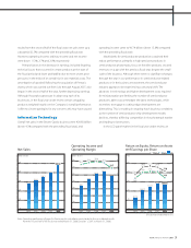
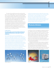
Liquid crystal displays (LCDs) permeate our lives on a broad scale,
from flat panel televisions and computer monitors to digital
cameras and mobile phones. LCD photomasks are the master
plates used in the manufacture of these LCD panels. Hoya is the
world’s leading producer of LCD photomasks, and it has strengths
in the production of large-scale LCD photomasks.
The LCD panel market continues to grow year by year, driven
by demand for large flat-panel televisions and computers.
Particularly in flat-panel televisions, which have enjoyed explosive
global popularity, the panel manufacturers that are the Company’s
customers are working to increase panel size and improve
productivity, in response to demand for larger displays and an
ongoing rapid slide in unit product prices. In line with such trends,
Hoya strives to provide large-scale photomasks for the efficient
manufacture of larger panels and continues to supply new
technologies that help improve its customers’ productivity.
LCD Photomasks
Hoya supports the expansion of the market
for LCD panels
Highlights
EUV mask blanks, regarded as a candidate for the
next generation of lithography technology
Policies and Forecasts for the Year Ahead
Large-scale photomasks for LCD production
HOYA ANNUAL REPORT 2008 13