Pentax 2008 Annual Report Download - page 14
Download and view the complete annual report
Please find page 14 of the 2008 Pentax annual report below. You can navigate through the pages in the report by either clicking on the pages listed below, or by using the keyword search tool below to find specific information within the annual report.-
 1
1 -
2
-
3
-
 4
4 -
 5
5 -
 6
6 -
 7
7 -
 8
8 -
 9
9 -
 10
10 -
 11
11 -
 12
12 -
 13
13 -
 14
14 -
 15
15 -
 16
16 -
 17
17 -
 18
18 -
 19
19 -
 20
20 -
 21
21 -
 22
22 -
 23
23 -
 24
24 -
25
-
26
-
27
-
28
-
29
-
30
-
31
-
32
-
33
-
34
-
35
-
36
-
37
-
38
-
39
-
40
-
41
-
42
-
43
-
44
-
45
-
46
-
47
-
48
-
49
-
50
-
51
-
52
-
53
-
54
-
55
-
56
-
57
-
58
-
59
-
60
-
61
-
62
-
63
-
64
-
65
-
66
-
67
-
68
-
69
-
70
-
71
-
72
-
73
-
74
-
75
-
76
-
77
-
78
-
79
-
80
-
81
-
82
-
83
-
84
-
85
-
86
-
87
-
88
-
89
-
90
-
91
-
92
 |
 |

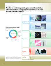
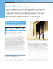
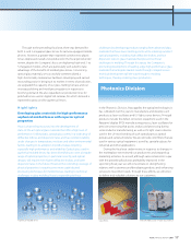
Electro-Optics Division
As semiconductor miniaturization continues, lithographic
exposure—which transfers the circuit pattern onto the wafers—is
key to the production process. Hoya produces photomasks, which
are the master plates for the patterns used in lithographic
exposure, and the mask blanks that form the substrate for the
photomasks. A mask blank is a highly polished glass plate onto
which a homogeneous metallic film and photosensitizing agent
have been applied; a photomask is a mask blank onto which a
pattern has been drawn with an electron beam or laser writing
device. Semiconductor manufacturers seek to continue
integrating more components with smaller circuits, as this
increases device performance and saves on raw materials costs.
Hoya takes advantage of its technical capabilities cultivated over
the years to support semiconductor miniaturization by providing
high-precision mask blanks and photomasks that competitors
cannot match.
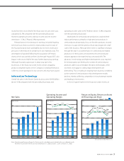
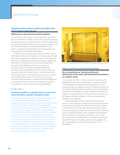
High-precision products drove sales
Looking back on the semiconductor market in the fiscal year
under review, while the first half saw hearty incentives for cutting-
edge development, the second half witnessed manufacturers
seeking to improve productivity while pursuing miniaturization
through more conservative means. At the same time, special
attention was placed on profitability and efficiency as alarms were
sounded over ever-inflating development investment costs.
In this environment, performance of Hoya’s mask blanks
stayed strong in the fiscal year under review, primarily supported
by high-precision products. Among these, phase-shift mask
blanks, which enable finer lines to be drawn by changing the
phase of the light used, sustained their growth trend from the
preceding year. The Company has nearly completed a technique
for drawing circuit lines 45 nm* in width and has commenced
product shipments, as well as steadily progressing in
development of the upcoming 32 nm line width products.
In photomasks, rather than pursuing scale of business Hoya
concentrated on developing frontline applications and
strengthening cost competitiveness. As a result, we sustained the
same level of profitability as during the preceding year. In the
Along with the digitization of telecommunications, broadcasting, home electronics, entertainment
and a host of other content comes the need to develop technologies to process increasing volumes
of data at high speeds. Hoya provides the technology and products that enable the development
of higher-capacity, faster information and telecommunications equipment that is more compact
and lightweight. In the process, we make a significant contribution to the onward march of
large-screen FPD televisions, digital cameras, notebook PCs and other digital products.
Information Technology
Mask Blanks and Photomasks
for Semiconductor Production
Hoya provides high-value-added products
and services that aid in semiconductor
miniaturization and process enhancement
Significant Actions Taken and Results Achieved in
the Fiscal Year under Review
From left: a glass substrate, a phase-shift half-tone mask blank, a homogenous metallic film
coated layer, a completed blank with photoresist coating and a complete photomask with
circuit
12