Samsung 2013 Annual Report Download - page 14
Download and view the complete annual report
Please find page 14 of the 2013 Samsung annual report below. You can navigate through the pages in the report by either clicking on the pages listed below, or by using the keyword search tool below to find specific information within the annual report.-
 1
1 -
2
-
3
-
 4
4 -
 5
5 -
 6
6 -
 7
7 -
 8
8 -
 9
9 -
 10
10 -
 11
11 -
 12
12 -
 13
13 -
 14
14 -
 15
15 -
 16
16 -
 17
17 -
 18
18 -
 19
19 -
 20
20 -
 21
21 -
 22
22 -
 23
23 -
 24
24 -
25
-
26
-
27
-
28
-
29
-
30
-
31
-
32
-
33
-
34
-
35
-
36
-
37
-
38
-
39
-
40
-
41
-
42
-
43
-
44
-
45
-
46
-
47
-
48
-
49
-
50
-
51
-
52
-
53
-
54
-
55
-
56
-
57
-
58
 |
 |
24 25
2013 SAMSUNG ELECTRONICS ANNUAL REPORT
crosstalk. Other key accomplishments include the successful
development of 14-nanometer FinFET logic process and
design infrastructure for advanced mobile SoCs and
development of the industry’s first 45-nanometer eFlash
process technology.
In 2014, we will focus on improving product competitive-
ness while setting the groundwork for next-generation
14-nanometer process technology. To meet market demand
for advanced system semiconductor products, we will
continue to provide Total Mobile Solution, including APs,
ModAPs* and CMOS image sensors with the industry’s highest
performance and energy efficiency. We will also strengthen
support for our foundry customers.
DS
Device Solutions
With cutting-edge competitiveness in process technology and
advanced development of next-generation products, Samsung
Electronics has consistently expanded in the system LSI
business. We are currently maintaining our lead in the global
market with a focus on three key segments: mobile application
processors (APs) for smartphones, CMOS image sensors for
mobile cameras and the advanced foundry business.
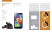
In 2013, Samsung pioneered innovation in mobile APs by
launching Exynos 5 Octa based on ARM®big.LITTLE™
technology with Heterogeneous Multi-Processing (HMP)
capability, which provides significant performance and power
efficiency improvements. In addition, Samsung launched
a lineup of CMOS image sensors based on ISOCELL
technology that enhances image quality and minimizes
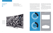
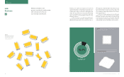
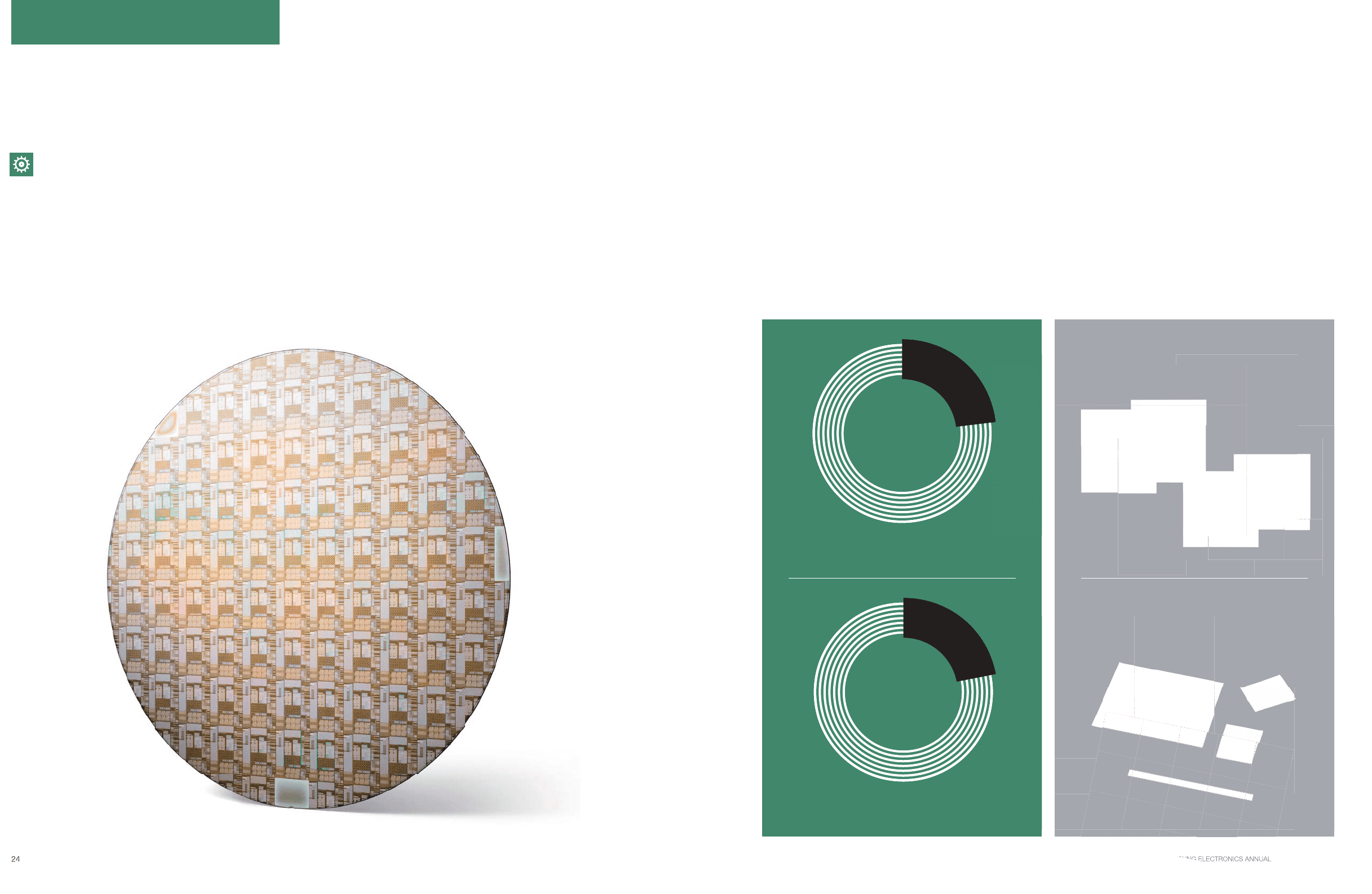
Top Global Smartcard IC (SIM)
Market Share in 2013
No. 2 Global CMOS Image Sensor
Market Share in 2013
23.0%
22.0%
Source: TSR, as of rst half of 2013 Source: ABI, as of rst half of 2013
*Samsung’s single chip solution integrating modem and AP together
Leading continuous innovation
in the electronics industry
with optimized system
semiconductor solutions
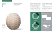
System LSI
Business
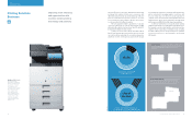
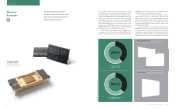
Smart Card IC, Display Driver IC Smart card IC with the industry’s
rst EAL7 security certi cation for a secure microcontroller and
mobile display driver IC for WQHD (Wide Quad HD) displays
fabricated with advanced 45-nanometer process technology.
Exynos 5 Octa, 16-Megapixel ISOCELL CMOS Image Sensor
High-performance and low-power mobile AP featuring
Heterogeneous Multi-Processing (HMP) technology and high-pixel
CMOS image sensor with ISOCELL technology.
14-nanometer LPE
(Low Power Early Version)
Process Technology
Next-generation process
technology with the industry’s
rst 3D architecture that
delivers up to 35% less power
consumption, 20% higher
performance and 15% chip
area reduction compared to
20-nanometer planar technology.