Pentax 2007 Annual Report Download - page 23
Download and view the complete annual report
Please find page 23 of the 2007 Pentax annual report below. You can navigate through the pages in the report by either clicking on the pages listed below, or by using the keyword search tool below to find specific information within the annual report.-
 1
1 -
2
-
3
-
4
-
5
-
6
-
7
-
8
-
9
-
10
-
11
-
12
-
 13
13 -
 14
14 -
 15
15 -
 16
16 -
 17
17 -
 18
18 -
 19
19 -
 20
20 -
 21
21 -
 22
22 -
 23
23 -
 24
24 -
 25
25 -
 26
26 -
 27
27 -
 28
28 -
 29
29 -
 30
30 -
 31
31 -
 32
32 -
 33
33 -
34
-
35
-
36
-
37
-
38
-
39
-
40
-
41
-
42
-
43
-
44
-
45
-
46
-
47
-
48
-
49
-
50
-
51
-
52
-
53
-
54
-
55
-
56
-
57
-
58
-
59
-
60
-
61
-
62
-
63
-
64
-
65
-
66
-
67
-
68
-
69
-
70
-
71
-
72
-
73
-
74
-
75
-
76
-
77
-
78
 |
 |

21
energy consumption, they are expected to offer lower production
costs thanks to the smaller size and lower weight of cooling
systems. The aim is to have the new technology incorporated into
high efficiency power devices across a variety of fields.
<Nanotechnology>
1. Nanoimprint technology
In such fields as semiconductors and data storage where the
market expects device features to continue to shrink, the
overriding objective is to cut costs by increasing data density.
One strategic solution on which work is proceeding involves
abandoning photolithography. Printing technologies form the
basis of this new approach, and especially at the nano level,
nanoimprint technologies are currently enjoying the limelight.
They involve first producing one ultra-fine mother mold, from
which is produced daughter and grandchild molds that can be
used to transfer the pattern by stamping. It is thought that this
will be the cheapest means of reproducing large numbers of
ultra-fine patterns. Hoya has already commenced efforts to
produce nanoimprint molds using its existing photomask and
mask blank production
technologies. The company
expects to realize practical
applications in such areas as
optical parts, next-generation
magnetic disks and
semiconductors.
2. Nanoparticles
Once certain materials are made on the nano scale, their
characteristics as materials alter, and new functions such as light
emission can be brought about. As an example, when gold is
made as fine as nanoparticles it becomes transparent to light.
Not only that—it also becomes red. Stained glass is one
example. This came about when, in ancient times, gold
nanoparticles were accidentally mixed with glass. Hoya is
currently undertaking R&D on the dispersion of a variety of
nanoparticles and changes in their surface characteristics, and
attempts are being made to develop compound materials with
new physical properties from a suitable combination of
nanoparticles. Based on work in progress, Hoya foresees
practical applications in materials for optical parts and data
storage related fields.
* Nano is used to mean one billionth of a meter.
<Optical Communications>
Hoya is engaged in the development of optical communications
parts and materials and special fiber optic cables, in anticipation of
future developments in fiber optic networks. In the midst of the
swift rollout of broadband internet connections, Hoya is continuing
to push ahead with R&D on FTTH (fiber to the home). For
example, Hoya is undertaking R&D on a key part that, once a fiber
optic cable is connected to it, would convert the optical signal to
an electrical one. Another R&D topic is a module that would boost
transmission speeds. In the optical communications field, Hoya is
actively investing in overseas venture businesses and undertaking
collaborative development. For example, Hoya has an alliance with
the U.S. firm Xponent Photonics, Inc., which owns technologies
for highly integrated optical modules.
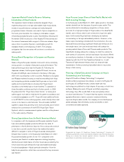
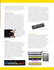
<EUV Mask Blanks>
In the semiconductor industry, the need for higher data density
and low energy consumption are behind the demand that
circuitry shrink even further. Under the Road Map for next-
generation lithography technology, extreme ultra violet (EUV)
light is regarded as the strongest candidate as an exposure light
source for semiconductor production. Hoya has already
completed its basic R&D for EUV mask blanks, and it has started
offering test blanks with a view to commencement of mass
production. In 2006, the R&D Center transferred responsibility
for the development of EUV mask blanks to the relevant
business division, which will henceforth be engaged in
development leading to practical applications.
Electrostatic chuck
Low thermal expansion glass
Multilayer (Si & Mo 40 layers)
Multilayer
Conducting layer
6.9 nm
Extreme ultra-violet light (13-14 nm)
Optical-waveguide type FTTH component
×1 nanoimprint template (mold) for
32 nm node production
Illustration of reflective EUV mask
Fluorescence of nanocrystalline indium phosphorus semiconductor