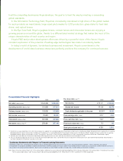
Pentax 2007 Annual Report Download - page 11
Download and view the complete annual report
Please find page 11 of the 2007 Pentax annual report below. You can navigate through the pages in the report by either clicking on the pages listed below, or by using the keyword search tool below to find specific information within the annual report.-
 1
1 -
 2
2 -
 3
3 -
 4
4 -
 5
5 -
 6
6 -
 7
7 -
 8
8 -
 9
9 -
 10
10 -
 11
11 -
 12
12 -
 13
13 -
 14
14 -
 15
15 -
 16
16 -
 17
17 -
 18
18 -
 19
19 -
 20
20 -
 21
21 -
 22
22 -
23
-
24
-
25
-
26
-
27
-
28
-
29
-
30
-
31
-
32
-
33
-
34
-
35
-
36
-
37
-
38
-
39
-
40
-
41
-
42
-
43
-
44
-
45
-
46
-
47
-
48
-
49
-
50
-
51
-
52
-
53
-
54
-
55
-
56
-
57
-
58
-
59
-
60
-
61
-
62
-
63
-
64
-
65
-
66
-
67
-
68
-
69
-
70
-
71
-
72
-
73
-
74
-
75
-
76
-
77
-
78
 |
 |

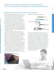
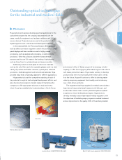
Mask blanks and photomasks are essential in the production of
semiconductor chips. They are the master plates used to transfer
the minute, highly complex circuit patterns for semiconductors
onto the wafers that become IC chips. A photomask is a
six-inch-wide glass plate onto which an electron beam or laser
writing device has drawn a circuit pattern. A mask blank is the
same plate before it has been written with a circuit pattern. Hoya
has several strengths in this field, including: (1) the superb
technologies it uses to precisely polish glass substrates and then
lay down homogeneous metallic films and photosensitizing agents
on those substrates; (2) the ability to develop new products that
exactly meet client needs, thanks to a collaborative development
project model: and (3) excellent production capabilities, which allow
the company to offer a stable supply of finished mask blanks and
photomasks to the market.
As semiconductors have evolved to offer ever greater
performance, and as circuit patterns have become increasingly
complex, semiconductor design rules*1 are steadily changing to
require ever more precise line width, from 90 nm*2 through 65 nm
to 45-32 nm. During the fiscal year ended March 31, 2007,
demand for Hoya’s high-end products continued to expand. In
particular, very strong growth was seen in sales of phase-shift
mask blanks, which are produced by taking advantage of the phase
difference of light rays to realize higher resolution on the
semiconductor wafer. Hoya will continue to develop leading-edge
technologies through its collaborative development programs with
manufacturers of semiconductors and masks. It will also further
enhance its production systems to ensure that client expectations
are met, and will endeavor to further reduce production costs.
In the photomask business, Hoya is devoting its efforts to the
development and production of high-precision products, focusing
on high-end items. During the year, Hoya shipped increasing
quantities of photomasks compatible with 65 nm node production,
and shipments of photomasks for use in development of next-
generation 45 nm node production were also rolled out. The light
source used for the lithographic exposure of circuit patterns onto
semiconductor wafers is in the process of moving from krypton
fluoride (KrF) with a wavelength of 248 nm, to the argon fluoride
(ArF) excimer laser, with a wavelength of 193 nm. Additionally,
through the use of immersion technology*3 and ArF light sources, it
has been possible to achieve line widths of 32 nm and below. For
leading-edge applications, not only semiconductor manufacturers,
but also photomask makers, require high level technologies, and
there are only a limited number of mask suppliers that are able to
meet those needs. Given this situation, Hoya’s engineering and
production divisions will work as one, doing their utmost for the
further development of high-precision photomasks that meet
market needs, all the while keeping a close watch on future
technological developments.
Transfer image of circuit pattern in the exposure process
Reduced projection
lens unit
Photomask
Light source
Condenser lens
Wafer
(
Semiconductor chip
)
Mask blank (left) and photomask (right)
9
●Electro-Optics
Hoya’s Global Network
Aiming for the ultimate in performance and functionality,
Hoya is committed to developing new leading-edge technologies
Mask Blanks and Photomasks for Producing Semiconductors
Mask Blanks and Photomasks for Producing SemiconductorsElectro-Optics Division
*1. Design rules are constraints placed on the design of LSIs to ensure that
production processes can successfully meet the design intent.
*2. A nanometer (nm) is one billionth of a meter.
*3. With immersion technology, the gap between the projection lens and the wafer is
filled with a liquid to improve resolution.