Pentax 2005 Annual Report Download - page 14
Download and view the complete annual report
Please find page 14 of the 2005 Pentax annual report below. You can navigate through the pages in the report by either clicking on the pages listed below, or by using the keyword search tool below to find specific information within the annual report.-
 1
1 -
2
-
3
-
 4
4 -
 5
5 -
 6
6 -
 7
7 -
 8
8 -
 9
9 -
 10
10 -
 11
11 -
 12
12 -
 13
13 -
 14
14 -
 15
15 -
 16
16 -
 17
17 -
 18
18 -
 19
19 -
 20
20 -
 21
21 -
 22
22 -
 23
23 -
 24
24 -
25
-
26
-
27
-
28
-
29
-
30
-
31
-
32
-
33
-
34
-
35
-
36
-
37
-
38
-
39
-
40
-
41
-
42
-
43
-
44
-
45
-
46
-
47
-
48
-
49
-
50
-
51
-
52
-
53
-
54
-
55
-
56
-
57
-
58
-
59
-
60
-
61
-
62
-
63
-
64
-
65
-
66
-
67
-
68
-
69
-
70
-
71
-
72
-
73
-
74
-
75
-
76
-
77
-
78
-
79
 |
 |
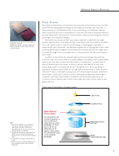
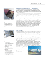
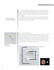
Photomasks Used in the Production of Semiconductors
In the semiconductor production process, the photomask plays a role similar to that of a
negative film in photography. There are strong synergies between the development of mask
blanks for semiconductors and the photomasks used for LCD panel production, and this is one
of Hoya’s key business platforms.
In fiscal 2005, the demand for semiconductors fell steeply from summer onward, and this led
to a slowing in demand for low-end masks. On the other hand, however, the development of
leading-edge technologies by semiconductor manufacturers is proceeding at a healthy pace, and
high-end photomasks continued to post firm growth. In leading-edge products, Hoya has already
commenced the supply of masks for mass production meeting the 90-nm and 65-nm design
rules, and expects that the trend toward increasingly fine tolerances will continue into the future.
Lithography based on an ArF excimer light source*1 is becoming the norm for the mass
production of semiconductors, and by taking advantage of immersion technologies*2, the
potential for this light source to continue to be used for future-generation production processes
is increasing. This approach, while allowing for the continued relevance of existing lithography
equipment, will also give rise to the need for a photomask with the capacity to respond to next-
generation lithography technologies. Thus, the importance of developing leading-edge masks
continues to grow. In a market characterized by increasingly fierce competition, Hoya will
continue to stress the development and production of high value-added products, while
maintaining its close collaborative relationships with industry partners.
Notes:
*1. Argon fluoride, wavelength 193 nm.
*2. This is a next-generation lithographic
technology. The gap between the lens and
the wafer is filled with a liquid, which
improves the resolution of the etching
process.
Notes:
*1. Fifth-generation:
A mother glass plate of
1,100 mm x 1,300 mm, which yields
three 32-inch wide LCD televisions panels.
Sixth-generation:
A mother glass plate measuring
1,500 mm x 1,850 mm, which yields
eight 32-inch LCD television panels.
Seventh generation:
A mother glass plate of
1,870 mm x 2,200 mm, which yields
twelve 32-inch LCD television panels,
or three 50-inch LCD television panels.
Eighth generation:
A mother glass plate measuring
2,160 mm x 2,400 mm, which yields
six 50-inch LCD television panels.
*2. Gray tone mask:
A mask that produces an intermediate layer
(gray tone) from light interference and the
diffraction effect. Use of this mask reduces
the number of lithographic processes of TFT
LCD panels from five to four.
Electro-Optics Division
Taiwan plant
Photomask for the production of semiconductors
(front)
LCD photomask
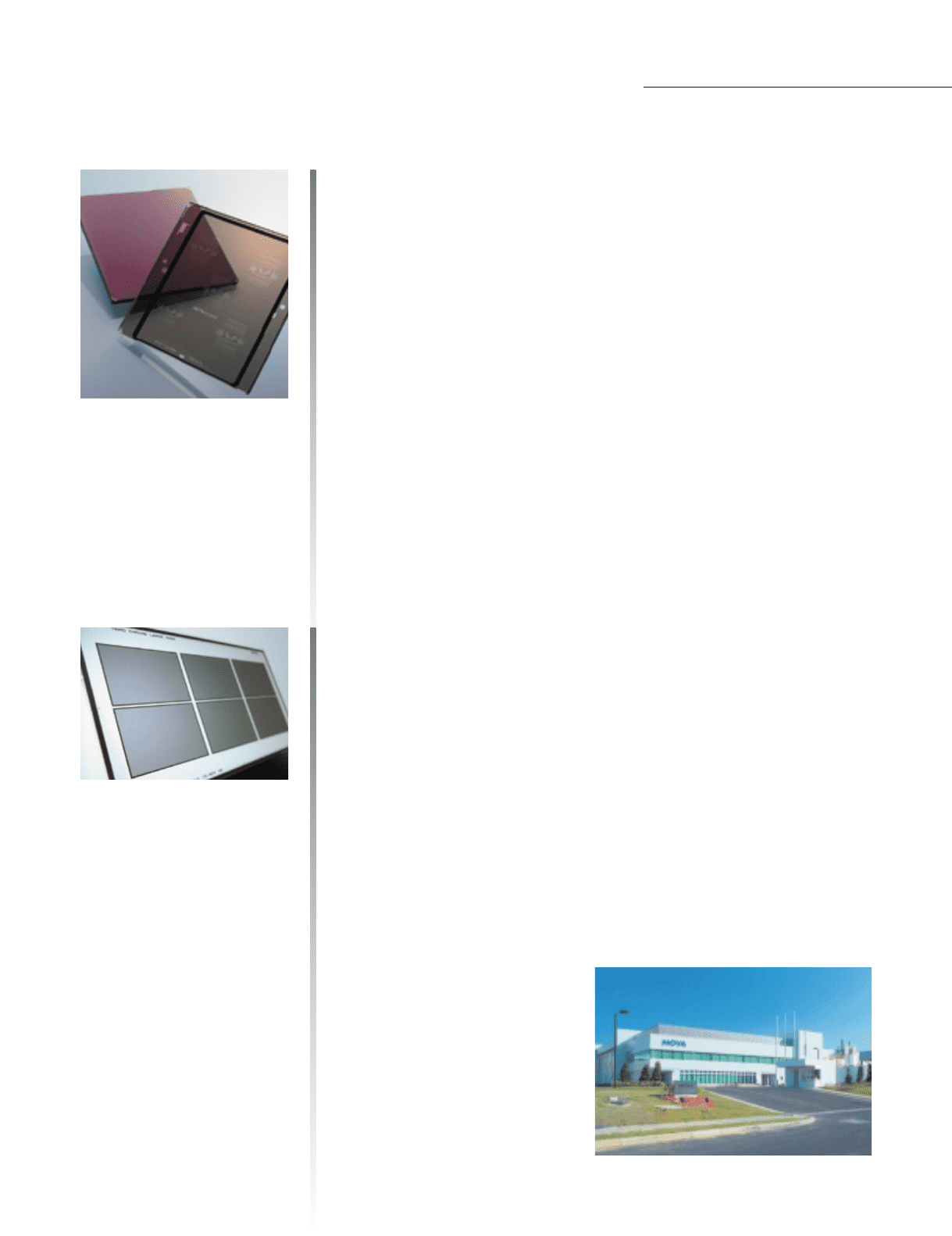
LCD Photomasks
LCD photomasks are the master plates inscribed with the patterns needed for the production
of LCD display panels, such as those used in LCD televisions and computer monitors. Today’s
trend has LCD televisions increasing in size every year. Hoya takes pride in its ability to produce
the large-scale LCD photomasks required, and continues to demonstrate a clear technological
advantage in this field.
During the fiscal year under review, Hoya proceeded with plans to open new LCD
photomask plants in Taiwan (which began operation in January 2005) and South Korea, to
ensure that it could continue to respond to increasing demand and meet the needs of large-
scale flat panel manufacturers. Currently, common panel sizes for large-scale televisions are the
fifth- and sixth-generation sizes*1, but Hoya’s new plants in Taiwan and South Korea are for the
production of photomasks for seventh- and eighth-generation panel sizes.
There is no doubt that the rate of adoption of LCD televisions in the market is increasing,
both because consumers are replacing their cathode ray tube (CRT)-based TVs with LCD TVs,
and because of the increase in demand for larger televisions. However, to further stimulate
demand, it is widely believed that a reduction in production cost is imperative. Hoya has
developed a gray tone mask*2 ahead of its competitors. This high-value-added mask reduces the
number of steps in the production of LCD
panels and increases the yield rate, helping
manufacturers to enhance production
efficiencies. Hoya will continue to pursue
technological innovation and assist in the
effort to improve the market acceptance of
LCD-related products.