Pentax 2005 Annual Report Download - page 13
Download and view the complete annual report
Please find page 13 of the 2005 Pentax annual report below. You can navigate through the pages in the report by either clicking on the pages listed below, or by using the keyword search tool below to find specific information within the annual report.-
 1
1 -
2
-
 3
3 -
 4
4 -
 5
5 -
 6
6 -
 7
7 -
 8
8 -
 9
9 -
 10
10 -
 11
11 -
 12
12 -
 13
13 -
 14
14 -
 15
15 -
 16
16 -
 17
17 -
 18
18 -
 19
19 -
 20
20 -
 21
21 -
 22
22 -
 23
23 -
24
-
25
-
26
-
27
-
28
-
29
-
30
-
31
-
32
-
33
-
34
-
35
-
36
-
37
-
38
-
39
-
40
-
41
-
42
-
43
-
44
-
45
-
46
-
47
-
48
-
49
-
50
-
51
-
52
-
53
-
54
-
55
-
56
-
57
-
58
-
59
-
60
-
61
-
62
-
63
-
64
-
65
-
66
-
67
-
68
-
69
-
70
-
71
-
72
-
73
-
74
-
75
-
76
-
77
-
78
-
79
 |
 |
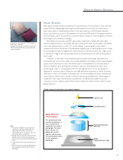
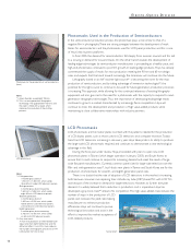
Mask Blanks
Mask blanks and photomasks are essential for the production of semiconductor chips and LCD
panels. With the leading-edge technologies and the expertise it has built over many years in
these areas, Hoya is a fundamental partner to the semiconductor and LCD panel industries.
Hoya is particularly proud of its achievement of a more than 70% share of the global market for
the mask blanks used in the production of semiconductors, driven by client recognition of Hoya’s
technological and competitive strengths.
Mask blanks are precisely polished*1 glass plates coated with a metallic film and a light-
sensitive material (resist). A mask blank becomes a photomask when circuit patterns are etched
into it with electron beams or lasers. To use the analogy of a photograph, a mask blank is
unexposed film, and a photomask is the developed negative. Just as a photographic print is made
by passing light through the negative, the semiconductor production process uses a light source
to transfer the image of the circuit pattern that is on the photomask onto the semiconductor’s
silicon wafer.
In addition to the need for the extremely high-resolution technologies that permit the
accurate transfer to the silicon wafer of a minutely detailed circuit pattern, clients require flawless
quality control that does not allow the tiniest scratch or the adherence of a minute speck of
dust. As LSI performance and capacity continue to improve, client demand for even more
precise design rules*2 is increasing, from 90 nm*3, through 65 nm to 45 nm, and demand is
expected to continue to grow further for such high-performance products as blanks for phase
shift masks*4. Hoya is committed to playing its part in the technological revolution faced by the
semiconductor industry, and is actively involved in developing next-generation technologies in
cooperation with major semiconductor manufacturers and photomask makers. Hoya will
continue to strive to develop state-of-the-art technologies that meet its clients’ needs for ever-
greater precision.
Notes:
*1. The surface roughness of a mask blank
must be no more than one billionth of a
meter (one nanometer), and must be
polished flat with an accuracy of less than
one thousandth of a millimeter.
*2. Design rules are constraints placed on the
design of LSIs to ensure that production
processes can successfully meet the design
intent.
*3. A nanometer (nm) equals one billionth of a
meter.
*4. Phase shift masks use phase differences in
light to enable extremely high-resolution
lithography.
Mask blanks for production of semiconductors
(Left) Glass substrate
(Middle) Glass plates coated with metallic film
(Right) Completed material coated with light-
sensitive material
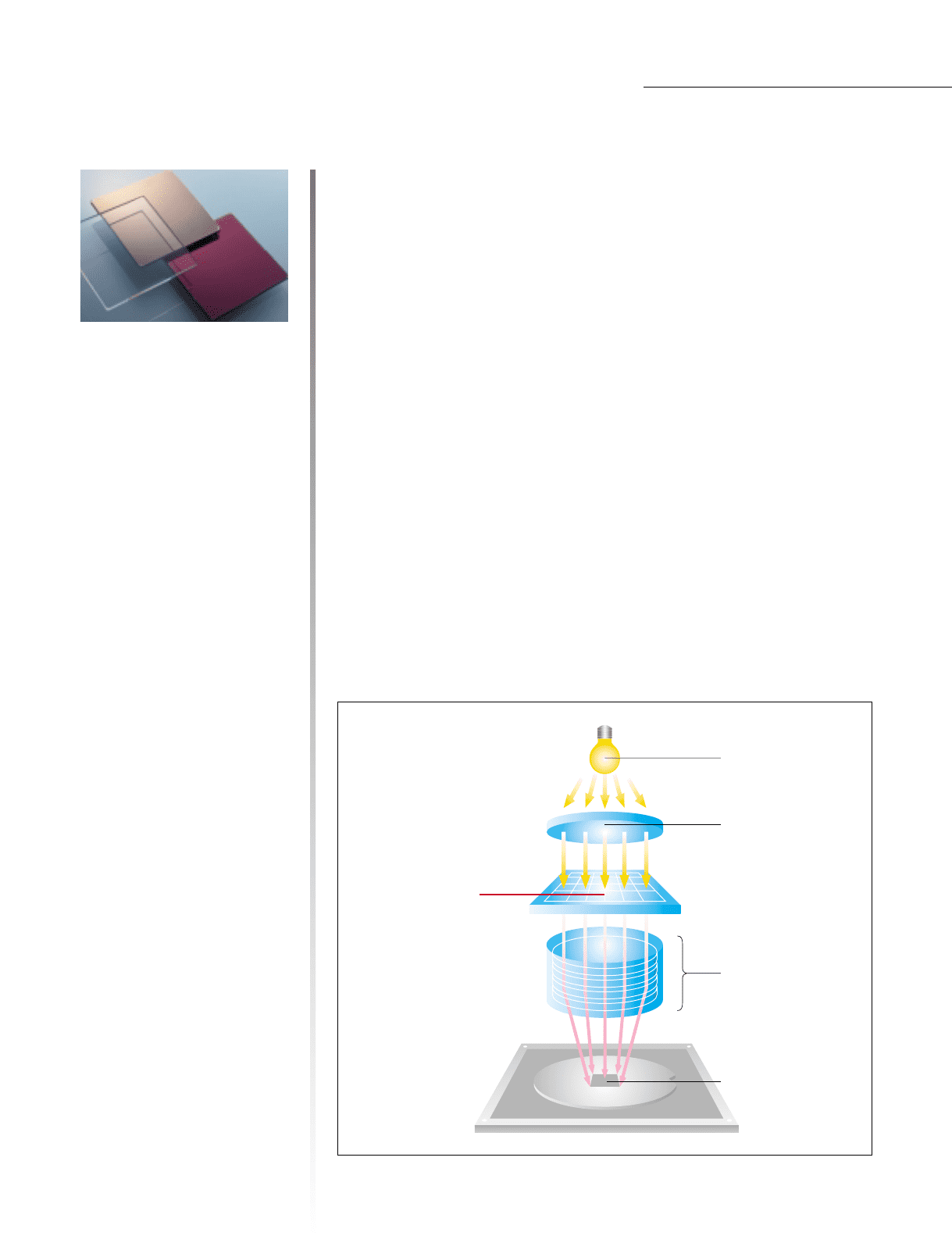
Electro-Optics Division
Transfer image of circuit pattern in the exposure process
Reduced projection
lens unit
Condenser lens
Mask Blanks/
Photomasks
The semiconductor chip
manufacturing process is
easy to understand if
compared to the world of
photography. The mask
blank is the film, the
photomasks are the
negative, and the wafers
(the semiconductor chips)
are the completed
photographs.
Light source