Pentax 2006 Annual Report Download - page 16
Download and view the complete annual report
Please find page 16 of the 2006 Pentax annual report below. You can navigate through the pages in the report by either clicking on the pages listed below, or by using the keyword search tool below to find specific information within the annual report.-
 1
1 -
2
-
3
-
4
-
5
-
 6
6 -
 7
7 -
 8
8 -
 9
9 -
 10
10 -
 11
11 -
 12
12 -
 13
13 -
 14
14 -
 15
15 -
 16
16 -
 17
17 -
 18
18 -
 19
19 -
 20
20 -
 21
21 -
 22
22 -
 23
23 -
 24
24 -
 25
25 -
 26
26 -
27
-
28
-
29
-
30
-
31
-
32
-
33
-
34
-
35
-
36
-
37
-
38
-
39
-
40
-
41
-
42
-
43
-
44
-
45
-
46
-
47
-
48
-
49
-
50
-
51
-
52
-
53
-
54
-
55
-
56
-
57
-
58
-
59
-
60
-
61
-
62
-
63
-
64
-
65
-
66
-
67
-
68
-
69
-
70
-
71
-
72
-
73
-
74
-
75
-
76
-
77
 |
 |

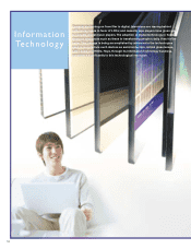
Information
Technology
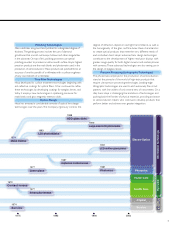
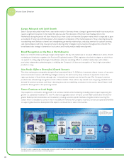
Transfer image of circuit pattern in the exposure process
Reduced projection
lens unit
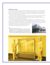
Photomasks for Producing Semiconductors
The market for photomasks used in the production of semiconductors is, on the
whole, in a period of stable growth. Industry participants, however, are closely
watching trends in restructuring on the supply side the industry as well as the day-
to-day changes in technological competitiveness. In this market environment, Hoya
devotes its resources to the development and production of high-precision
photomasks, concentrating on high-end products.
During the fiscal year ended March 31, 2006, full-scale commercial production
got under way for 65-nm photomasks. Since semiconductor manufacturers are
actively increasing their investment in R&D, Hoya also shipped samples of
state-of-the-art photomasks for use in the development of next-generation
semiconductors. The semiconductor industry is in the midst of a change in the light
source used for the lithographic etching of the circuit pattern onto the wafer, from
the current krypton fluoride (KrF) with a wavelength of 248 nm to the argon
fluoride (ArF) excimer laser with a wavelength of 193 nm. Furthermore, through
the use of immersion technology*4, ArF lasers have entered the ultra-high
resolution lithographic field, creating the possibility of line widths of 32 nm and
below. The demand for high-resolution photomasks grows stronger all the time, and
the Company expects its role in filling that demand to continue to expand.
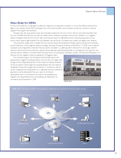
Mask Blanks for Producing Semiconductors
Mask blanks and photomasks are essential in the production of semiconductor chips. Mask blanks are precisely polished glass
plates coated with a metallic film and a light-sensitive material. A mask blank becomes a photomask when circuit patterns are
etched into it with electron beam or laser etching equipment. To use the analogy of film photography, the mask blank is like the
unexposed film, and the photomask is the equivalent of the developed negative. Just as a photographic print is made by passing
light through the negative onto the photographic paper, in semiconductor production a lithographic process is used to transfer
the circuit pattern on the photo mask onto the semiconductor wafer.
During the fiscal year ended March 31, 2006, Hoya’s high-end mask blanks, including phase-shift mask blanks*1, recorded big
increases in shipments due to the trend toward increased in
performance and capacity in large-scale integrated circuits
(LSIs). Semiconductor design rules*2 are steadily developing
to require ever more minute line widths, from 90 nm*3
through 65 nm to 45–32 nm. This trend means that mask
blanks will be required to offer a level of quality and
precision that exceeds current concepts of high resolution
and freedom from defects. The Company enjoys a more
than 70% share of the global market for mask blanks used
in semiconductor manufacture. As the leader in this field,
Hoya actively pursues technological innovation that will
result in product quality that is not only better than what
the competition can offer, but that also meets the absolute
quality requirements of clients. The Company will continue
to pour its energies into the development of leading-edge
technologies that meet clients’ needs by working
collaboratively with semiconductor manufacturers and
mask makers.
Electro-Optics Division
Light source
Condenser lens
Wafer
(
Semiconductor chip
)
Mask blanks/
photomasks
Notes:
*1. Phase-shift masks use phase differences in light to enable extremely high-resolution lithography.
*2. Design rules are constraints placed on the design of LSIs to ensure that production processes
can successfully meet the design intent.
*3. A nanometer (nm) equals one billionth of a meter.
*4. Using this lithographic technology, the gap between the lens and the wafer is filled with a liquid to
improve resolution.