Pentax 2013 Annual Report Download - page 31
Download and view the complete annual report
Please find page 31 of the 2013 Pentax annual report below. You can navigate through the pages in the report by either clicking on the pages listed below, or by using the keyword search tool below to find specific information within the annual report.-
 1
1 -
2
-
3
-
4
-
5
-
6
-
7
-
8
-
9
-
10
-
11
-
12
-
13
-
14
-
15
-
16
-
17
-
18
-
19
-
20
-
 21
21 -
 22
22 -
 23
23 -
 24
24 -
 25
25 -
 26
26 -
 27
27 -
 28
28 -
 29
29 -
 30
30 -
 31
31 -
 32
32 -
 33
33 -
 34
34 -
 35
35 -
 36
36 -
 37
37 -
 38
38 -
 39
39 -
 40
40 -
 41
41 -
42
-
43
-
44
-
45
-
46
-
47
-
48
-
49
-
50
-
51
-
52
-
53
-
54
-
55
-
56
-
57
-
58
-
59
-
60
-
61
-
62
-
63
-
64
-
65
-
66
-
67
-
68
-
69
-
70
-
71
-
72
-
73
-
74
-
75
-
76
-
77
-
78
-
79
-
80
-
81
-
82
 |
 |
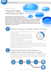
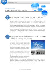
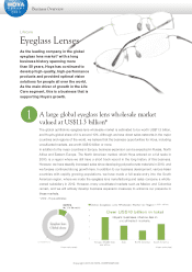
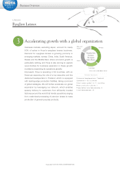
Business Overview
Copyright 2013 © HOYA CORPORATION
3
4
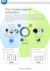
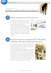
Global organization, risk diversification
Expectations that next-generation EUV lithography
technology will achieve further miniaturization
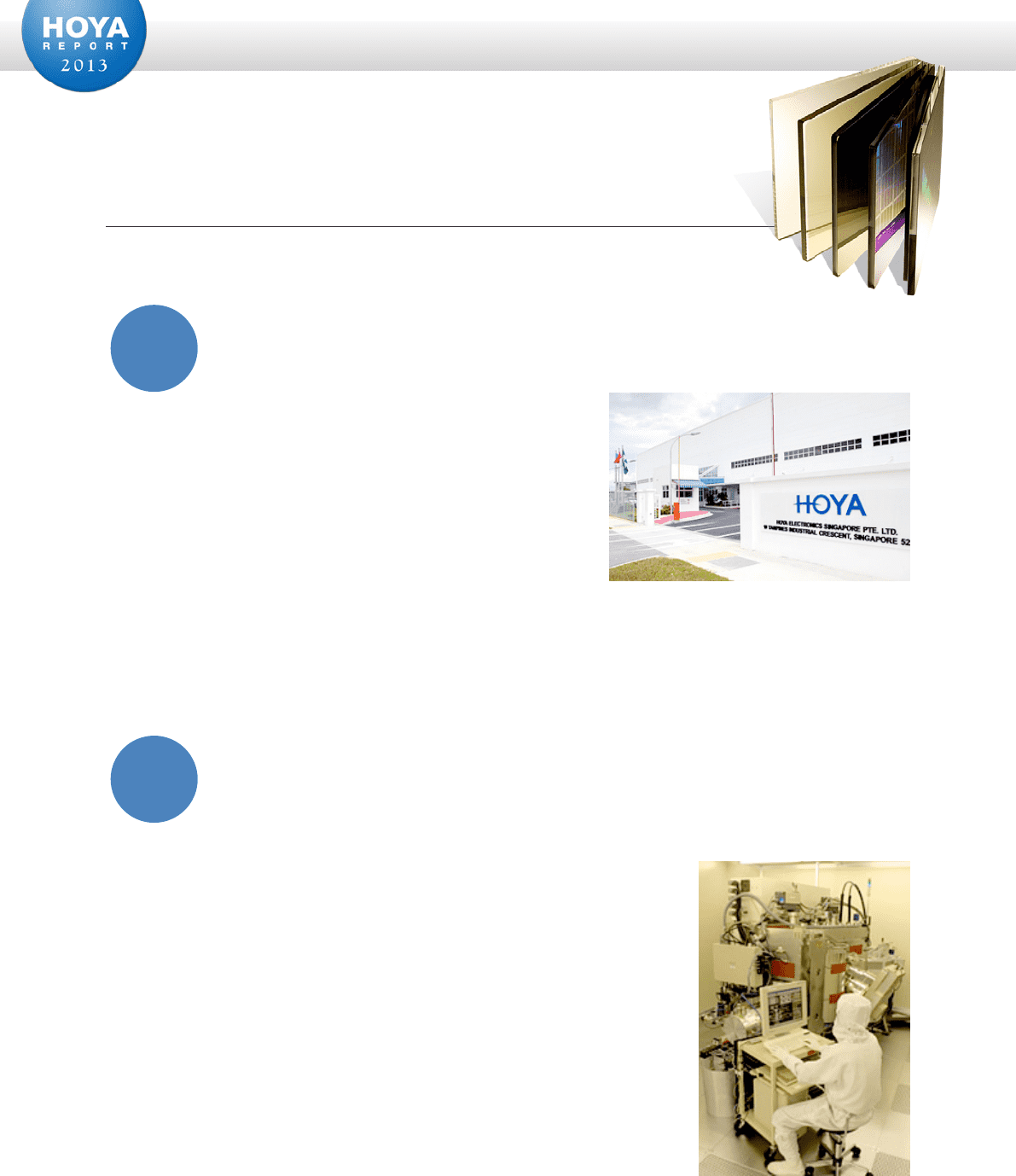
Singapore Plant
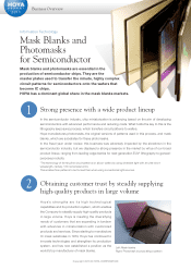
Mask Blanks and Photomasks for Semiconductor
Information Technology
In response to the Great East Japan Earthquake,
Hoya constructed a new plant in Singapore and put
it into operation in September 2012 to enhance
production efficiency and diversify risks.
Going forward, together with the Nagasaka Plant in
Japan, Hoya will promote R&D in cutting-edge fields
and build an efficient production system that handles
high-precision products to ge neral-purpose
products. Moreover, Hoya plans to expand business
under an organization that can supply high-quality
products to customers more rapidly and steadily
than before.
Chip miniaturization requires smoothness and flatness at a level
of more than ten nanometers with no defects in mask blanks as
well. Further miniaturization of semiconductors is a growth driver
for Hoya, which handles high-end products.
In the semiconductor industry, the development of light sources
used in the lithography process has advanced from conventional
ArF (wavelength of 193nm) to EUV (extreme ultraviolet light,
wavelength of 13-14nm), which can draw even finer patterns.
Hoya is also promoting the development of products suited to
EUV lithography at a rapid pace and has already started to supply
mask blanks for development use ahead of its competitors.
Hoya will continue to contribute to the miniaturization of
semiconductors as the leading supplier of mask blanks.