Pentax 2013 Annual Report Download - page 30
Download and view the complete annual report
Please find page 30 of the 2013 Pentax annual report below. You can navigate through the pages in the report by either clicking on the pages listed below, or by using the keyword search tool below to find specific information within the annual report.-
 1
1 -
2
-
3
-
4
-
5
-
6
-
7
-
8
-
9
-
10
-
11
-
12
-
13
-
14
-
15
-
16
-
17
-
18
-
19
-
 20
20 -
 21
21 -
 22
22 -
 23
23 -
 24
24 -
 25
25 -
 26
26 -
 27
27 -
 28
28 -
 29
29 -
 30
30 -
 31
31 -
 32
32 -
 33
33 -
 34
34 -
 35
35 -
 36
36 -
 37
37 -
 38
38 -
 39
39 -
 40
40 -
41
-
42
-
43
-
44
-
45
-
46
-
47
-
48
-
49
-
50
-
51
-
52
-
53
-
54
-
55
-
56
-
57
-
58
-
59
-
60
-
61
-
62
-
63
-
64
-
65
-
66
-
67
-
68
-
69
-
70
-
71
-
72
-
73
-
74
-
75
-
76
-
77
-
78
-
79
-
80
-
81
-
82
 |
 |

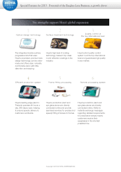
Business Overview
Copyright 2013 © HOYA CORPORATION
Mask Blanks and
Photomasks
for Semiconductor
Mask blanks and photomasks are essential in the
production of semiconductor chips. They are the
master plates used to transfer the minute, highly complex
circuit patterns for semiconductors onto the wafers that
become IC chips.
HOYA has a dominant global share in the mask blanks markets.
Information Technology
1
2
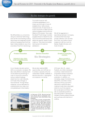
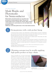
Strong presence with a wide product lineup
Obtaining customer trust by steadily supplying
high-quality products in large volume
In the semiconductor industry, chip miniaturization is advancing based on the aim of developing
semiconductors with advanced performance and reducing costs. What holds the key to this is the
lithography (exposure) process, which transfers circuit patterns to wafers.
Hoya manufactures photomasks, the original versions of patterns used in this process, and mask
blanks, which are substrates for these photomasks.
In the fiscal year under review, this business was adversely impacted by the slowdown in the
semiconductor industry, but we displayed a strong presence in the market by virtue of our broad
product lineup, ranging from leading-edge blanks for next-generation EUV* lithography to general-
purpose products.
*The technology of forming fine circuit patterns on silicon wafers by using ultraviolet light with an ultra-short
wavelength, namely, 13.5 nanometers (nm).
This enables finer patterns to be formed than when using conventional light sources.
Left: Mask blanks
Right: Photomask incorporating a pattern
Hoya's stre ng ths a re i ts h ig h technologica l
capabilities and its production system, which enables
the Company to steadily supply high-quality products
in large volume. Hoya is meeting the diversifying
needs of customers that are expanding in tandem
with advances in miniaturization with customized
products and services. Since starting to manufacture
IC mask substrates in 1974, Hoya has continued to
innovate technologies and strengthen its production
system, and has now established a position as the
world's top manufacturer of mask blanks.