Pentax 2003 Annual Report Download - page 9
Download and view the complete annual report
Please find page 9 of the 2003 Pentax annual report below. You can navigate through the pages in the report by either clicking on the pages listed below, or by using the keyword search tool below to find specific information within the annual report.-
 1
1 -
 2
2 -
 3
3 -
 4
4 -
 5
5 -
 6
6 -
 7
7 -
 8
8 -
 9
9 -
 10
10 -
 11
11 -
 12
12 -
 13
13 -
 14
14 -
 15
15 -
 16
16 -
 17
17 -
 18
18 -
 19
19 -
 20
20 -
21
-
22
-
23
-
24
-
25
-
26
-
27
-
28
-
29
-
30
-
31
-
32
-
33
-
34
-
35
-
36
-
37
-
38
-
39
-
40
-
41
-
42
-
43
-
44
-
45
-
46
-
47
-
48
-
49
-
50
-
51
-
52
-
53
-
54
-
55
-
56
-
57
-
58
-
59
-
60
-
61
-
62
-
63
-
64
-
65
-
66
 |
 |
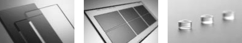
LCD Photomasks
As LCD televisions get larger and the use
of LCD displays for PCs becomes more
widespread, there is a growing need for
cost-effective production of LCD panels.
Hoya’s technological expertise with
large-scale photomasks, particularly
meter-long masks that can produce six
display panels at once, has won it a large
share of the market.
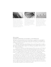
Glass Substrates and Mask
Blanks for Semiconductors
The perfectly polished substrate in the
foreground is a clear glass panel 15cm
square and 7mm thick. Coated with a
metallic layer and a resist it becomes the
mask blank pictured in the background.
Once the circuit patterns have been
exposed onto the surface with an elec-
tron beam it becomes a photomask. All
of these products have been well received
by semiconductor manufacturers.
Optical Glass and Lenses
Hoya produces a full range of optical
lenses, from imaging lenses used in video
and digital cameras to optical pickups
for DVD players and other devices. Its
cutting-edge production skill with
aspherical lenses helps make optical
devices smaller and lighter. Rising
demand is expected as more mobile tele-
phones and handheld devices incorporate
miniature cameras.
Electro-Optics
Mask Blanks and Photomasks for Semiconductors, and LCD Photomasks
Photomasks are the plates on which electronic circuit patterns are transferred to create semiconductor
chips. The clean material before the pattern is created is called a mask blank. To use photography as an
analogy, the mask blank is the unexposed film, the photomask is the exposed negative, and the semicon-
ductor chip is the printed picture.
Mask blanks consist of a precisely polished glass substrate coated with a metallic layer, which is
further coated with a photographic sensitive material known as the resist. Synthetic quartz is used for the
glass substrate, polished to a surface roughness of one million parts per millimeter, and a flatness of less
than 1,000 parts per millimeter.
The market for semiconductor mask blanks during fiscal 2002 was slow, due to the IT slump and
the accompanying adjustments to inventory. The market picked up during fiscal 2003, however, as cus-
tomers’ streamlining of operations and narrowing of product lineups began to taper off, and demand
increased for such high-performance products as phase shift masks. Hoya’s technical expertise with these
products is recognized around the world, allowing it to enjoy a 65% share of the global market.
Because the circuit patterns of semiconductor photomasks are exposed on to mask blanks with
electron beams or lasers, this exposure and the process to remove the extraneous material define the supe-
riority of the product. Price competitiveness is fierce in the market for low- and medium-quality products,
for which a great deal of technical skill is not required. This made for a difficult operating environment
for semiconductor photomasks, but bolstered by sales of Hoya’s high-quality products with a line width of
0.15 to 0.18 microns, sales remained on par with the previous fiscal year. Technical development that
keeps the Company ahead of the market is important to further increase its market share in this business.
Hoya has completed development of cutting-edge products with line widths of 0.09 to 0.13 microns, and
has already begun development on the next generation of products.
7
HOY A2003-e 0711 03.7.21 9:49 PM ページ 8