Samsung 2004 Annual Report Download - page 51
Download and view the complete annual report
Please find page 51 of the 2004 Samsung annual report below. You can navigate through the pages in the report by either clicking on the pages listed below, or by using the keyword search tool below to find specific information within the annual report.-
 1
1 -
2
-
3
-
4
-
5
-
6
-
7
-
8
-
9
-
10
-
11
-
12
-
13
-
14
-
15
-
16
-
17
-
18
-
19
-
20
-
21
-
22
-
23
-
24
-
25
-
26
-
27
-
28
-
29
-
30
-
31
-
32
-
33
-
34
-
35
-
36
-
37
-
38
-
39
-
40
-
 41
41 -
 42
42 -
 43
43 -
 44
44 -
 45
45 -
 46
46 -
 47
47 -
 48
48 -
 49
49 -
 50
50 -
 51
51 -
 52
52 -
 53
53 -
 54
54 -
 55
55 -
 56
56 -
 57
57 -
 58
58 -
 59
59 -
 60
60 -
 61
61 -
62
-
63
-
64
-
65
-
66
-
67
-
68
-
69
-
70
-
71
-
72
-
73
-
74
-
75
-
76
 |
 |
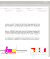
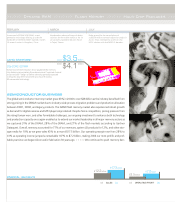
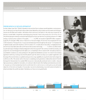
sities higher across-the-board in 2004 as we rolled out next-generation DDR2 SDRAM, multi-chip packages, and
OneNAND™flash memory solutions for the mobile device market. We bolstered our system LSI operations by
opening a new research lab in China and developing innovative new display driver ICs, CMOS image sensors,
and mobile processors. In the storage field, we continued to develop key components for the optical and mag-
netic storage devices that will store and retrieve digital content for tomorrow’s high-tech home and portable
entertainment devices. We also continued to sharpen our competitive edge on a more fundamental level by
adopting sub-micron process technology across all our product lines and developing revolutionary new design
tools and methodologies that will save development time and reduce costs as they dramatically shorten time-to-
market.
>>>>>
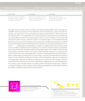
Our leadership over the past decade in a volatile commodity business like semiconductors is a testi-
mony to our ability to consistently pioneer new segments as we innovate to drive down production costs and diver-
sify our product portfolio by responding to high-end and specialized markets. As we marked our 30th anniversary
in the business on December 6, 2004, we announced an ambitious $24 billion investment in our production infra-
structure over the next six years to strategically position ourselves for emerging opportunities across the industry. In
2005, we will be stepping up development of nanotechnology to meet early market demand as we continue to
expand our product expertise and offerings in the system-on-chip, advanced logic, large-scale circuit integration,
and magnetic disk storage fields. We will also be accelerating work on efficient new memory design structures to
meet the performance requirements of tomorrow’s mobile devices and high performance computing applications.
This continuous cycle of innovation will give us a strategic portfolio of key patents that will serve as a catalyst for
convergence and synergy on both the product and technical levels, empowering us to create entirely new solutions
that will keep us solidly at the industry forefront in the years ahead.
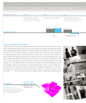
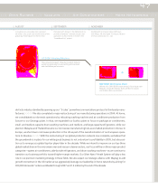
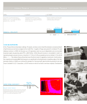
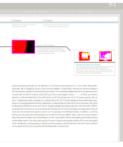
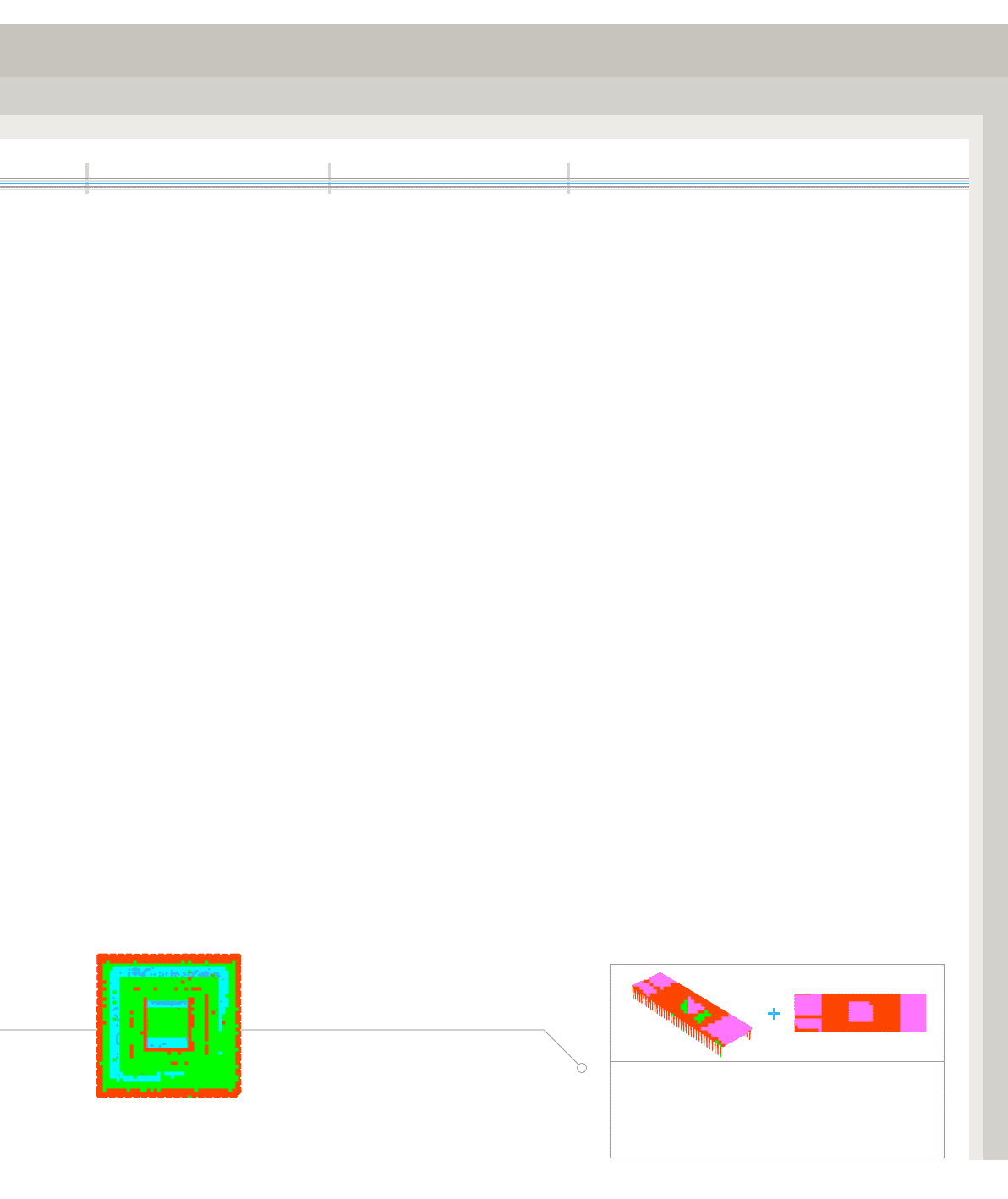
2.0-Megapixel CMOS Image Sensor
The industry’s first CMOS image sensor
fabricated with 0.13-micron technology provides
an ideal balance of size and resolution for
next-generation mobile devices.
>>> Display Driver ICs >>>>>>> CMOS Image Sensors >>>>>>> Mobile CPUs >>>>
8Gb NAND Flash Memory
We continued to lead in the mobile memory space by
developing the industry’s first 8-gigabit NAND flash memory
chip with 60-nanometer process technology, paving the way
for memory cards with capacities of up to 16-gigabytes.
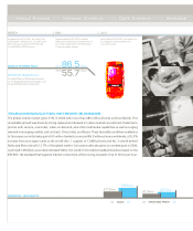
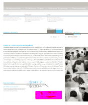
49
Announced the industry’s first 8Gb NAND
flash memory using 60nm technology, a 2Gb
DDR2 SDRAM using 80nm technology,
and a 667MHz mobile processor.
SEPTEMBER
Announced a 1Gb OneNAND™flash memory
using 90nm technology, a new unified
storage concept that combines fast NOR read
speeds with high NAND densities.
Marked our 30th anniversary in the
semiconductor business. Shipped the industry’s
first 512Mb GDDR3 DRAM for next-
generation graphics applications.
NOVEMBER DECEMBER