Pentax 2011 Annual Report Download - page 9
Download and view the complete annual report
Please find page 9 of the 2011 Pentax annual report below. You can navigate through the pages in the report by either clicking on the pages listed below, or by using the keyword search tool below to find specific information within the annual report.-
 1
1 -
 2
2 -
 3
3 -
 4
4 -
 5
5 -
 6
6 -
 7
7 -
 8
8 -
 9
9 -
 10
10 -
 11
11 -
 12
12 -
 13
13 -
 14
14 -
 15
15 -
 16
16 -
 17
17 -
 18
18 -
 19
19 -
 20
20 -
21
-
22
-
23
-
24
-
25
-
26
-
27
-
28
-
29
-
30
-
31
-
32
-
33
-
34
-
35
-
36
-
37
-
38
-
39
-
40
-
41
-
42
-
43
-
44
-
45
-
46
-
47
-
48
-
49
-
50
-
51
-
52
-
53
-
54
-
55
-
56
-
57
-
58
-
59
-
60
-
61
-
62
-
63
-
64
-
65
-
66
-
67
-
68
 |
 |
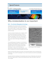
Why miniaturization is so important
Lithography is the process by which circuit patterns
with line width measured in nanometers are formed on
semiconductor wafers. This field, which is critical to
progress in semiconductor miniaturization, is Hoya’s
greatest strength.
Lasers are used as the light source in steppers, which
are machines that project microscopic circuitry on
wafers. The most advanced technology is ArF laser
immersion lithography, which uses a wavelength of
193nm. This technology can form lines only 40nm to
30nm wide, a level no other type of lithography can
match.
The accelerating pace of progress in circuit density is
placing increasing demands on the equipment used to
manufacture semiconductor devices. Only limited
potential remains for more progress with ArF laser
technology. To move on to the next step, the
semiconductor industry has turned its attention to EUV,
which is regarded as the ultimate lithography technology.
Extreme ultraviolet (EUV) light is the section of the ultraviolet spectrum with an extremely short
wavelength. In fact, the EUV wavelength of only 13.5nm is less than one-tenth the wavelengths
of ArF lasers.
Using light with this remarkably short wavelength opens the way to fabricating semiconductors
with an even higher density. Products that incorporate these chips will be faster, smaller and
more versatile.
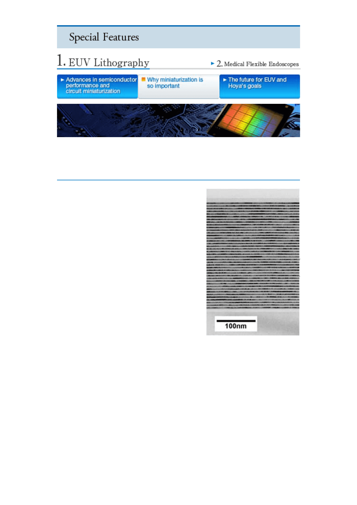
EUV – The ultimate lithography technology
Mo/Si multilayer for EUV lithography