Pentax 2011 Annual Report Download - page 52
Download and view the complete annual report
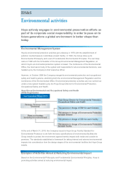
Please find page 52 of the 2011 Pentax annual report below. You can navigate through the pages in the report by either clicking on the pages listed below, or by using the keyword search tool below to find specific information within the annual report.-
 1
1 -
2
-
3
-
4
-
5
-
6
-
7
-
8
-
9
-
10
-
11
-
12
-
13
-
14
-
15
-
16
-
17
-
18
-
19
-
20
-
21
-
22
-
23
-
24
-
25
-
26
-
27
-
28
-
29
-
30
-
31
-
32
-
33
-
34
-
35
-
36
-
37
-
38
-
39
-
40
-
41
-
 42
42 -
 43
43 -
 44
44 -
 45
45 -
 46
46 -
 47
47 -
 48
48 -
 49
49 -
 50
50 -
 51
51 -
 52
52 -
 53
53 -
 54
54 -
 55
55 -
 56
56 -
 57
57 -
 58
58 -
 59
59 -
 60
60 -
 61
61 -
 62
62 -
63
-
64
-
65
-
66
-
67
-
68
 |
 |

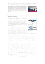
for analyzing and visualizing the optical phenomena of defects in phase-type diffractive lenses,
improving surface profilometry resolution with digital holography, and for measuring
transmittance in microscopic thin films. The department is also working to develop new optical
products.
Nanoimprint Technology:
Hoya is putting its lithographic technologies to use in the
development and trial production of nanoimprint molds, which
will be used in the creation of patterned media (DTM, BPM) fo
r
use in increasing the areal density of hard disk drives (HDDs),
and in high-brightness LEDs.
Various HDD manufacturers are vigorously pursuing R&D to
commercialize patterned media technology, and Hoya has
begun shipping DTM molds enabling nanoimprint processing on
all surfaces of 2.5-inch media. In BPM, Hoya has used the
latest microfabrication technologies to develop a mold
producing a bit pitch of 25 nanometers and surface recording
density of 1 Tbit/inch*.
In molds for use in manufacturing LEDs, the Company has
developed and started shipping samples of molds with 100–300
nanometer pitch size, suitable for high-brightness chip designs.
*Nanometer (nm):1 nanometer = 1 billionth of a meter
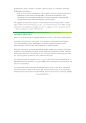
3C-SiC:
Hoya is promoting the development of 3C-SiC (cubic
monocrystal silicon carbide) semiconductor wafers and devices.
The superior energy efficiencies expected of this material
means it would be a counterweight to global warming when
applied in automobiles and home appliances such as air
conditioners. Hoya has reported at various international
conferences and symposia that it obtained very high channel
mobility of 200 cm2/Vs with a prototype 3C-SiC MOSFET
(metal oxide semiconductor field-effect transistor) it fabricated in fiscal 2011.
Optical Communications Parts:
A
s the FTTH (Fiber to the Home) environment widens around
the world, Hoya has developed a module for converting optical
signals to electrical ones at optical communication access
points that is compliant with GE-PON/G-PON2*, a high-speed
optical communications standard. By building a functional
device on top of a wafer, Hoya has succeeded in creating
products that are significantly smaller than existing products.
Hoya received approval from customers and launched product
shipments in fiscal 2011, and plans to ramp up mass production
in step with full-blown product acceptance in fiscal 2012. As optical networks continue to develop
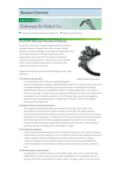
Nano-imprint mold for HDD
patterned media
Nano-imprint mold for high
intensity LED (x100,000)
3C-SiC
A
n optical telecommunications
device