Pentax 2011 Annual Report Download - page 30
Download and view the complete annual report
Please find page 30 of the 2011 Pentax annual report below. You can navigate through the pages in the report by either clicking on the pages listed below, or by using the keyword search tool below to find specific information within the annual report.-
 1
1 -
2
-
3
-
4
-
5
-
6
-
7
-
8
-
9
-
10
-
11
-
12
-
13
-
14
-
15
-
16
-
17
-
18
-
19
-
 20
20 -
 21
21 -
 22
22 -
 23
23 -
 24
24 -
 25
25 -
 26
26 -
 27
27 -
 28
28 -
 29
29 -
 30
30 -
 31
31 -
 32
32 -
 33
33 -
 34
34 -
 35
35 -
 36
36 -
 37
37 -
 38
38 -
 39
39 -
 40
40 -
41
-
42
-
43
-
44
-
45
-
46
-
47
-
48
-
49
-
50
-
51
-
52
-
53
-
54
-
55
-
56
-
57
-
58
-
59
-
60
-
61
-
62
-
63
-
64
-
65
-
66
-
67
-
68
 |
 |

Fiscal 2011 Business Overview and Results Outlook for Fiscal 2012
Fiscal 2011 Business Overview and Results
The year under review was marked by further progress in
semiconductor miniaturization and leading to increased activity
for mass production at the 45 nanometer node. At the same
time, consolidation among semiconductor makers at home and
abroad has resulted in fewer types of photomasks being used.
The market for mask blanks used in semiconductor production
grew steadily through 2007 but subsequently went through a
period of contraction amid worldwide economic stagnation until
2010, when demand recovered somewhat.
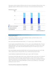
Such a backdrop contributed to Hoya’s mask blanks business in the volume shipped. In value
terms, however, sales declined year on year as a consequence of falling unit prices and
unfavorable exchange rates. Hoya faces continued competition in both cutting-edge and generic
products, but maintains a high share of the mask blanks market by virtue of an aggressive
approach to development, service and marketing.
A
mong semiconductor manufacturers there are mounting expectations that extreme ultraviolet
(EUV) lithography will prove a promising successor to ArF lithography currently in use for the
most complex devices. Hoya has been active in the R&D of mask blanks for use with EUV
lithography, and aims to ramp up trial production of EUV mask blanks soon.
Hoya was fortunate in that its Nagasaka Plant sustained no direct damage due to the Great East
Japan Earthquake. As a precaution against power restrictions in summer, the Company is
making back-up arrangements including facilities for in-house power generation.
Outlook for Fiscal 2012
Semiconductor makers are migrating to even finer process technologies; namely, 32 and 22
nanometers. As the leading manufacturer of mask blanks for semiconductor production, Hoya
will continue investing in R&D and manufacturing facilities with a view to satisfying the
technology and quality requirements of next-generation products.
Mask blanks for semiconductor
production
ANNUAL REPORT 2011