Pentax 2011 Annual Report Download - page 8
Download and view the complete annual report
Please find page 8 of the 2011 Pentax annual report below. You can navigate through the pages in the report by either clicking on the pages listed below, or by using the keyword search tool below to find specific information within the annual report.-
 1
1 -
 2
2 -
 3
3 -
 4
4 -
 5
5 -
 6
6 -
 7
7 -
 8
8 -
 9
9 -
 10
10 -
 11
11 -
 12
12 -
 13
13 -
 14
14 -
 15
15 -
 16
16 -
 17
17 -
 18
18 -
 19
19 -
20
-
21
-
22
-
23
-
24
-
25
-
26
-
27
-
28
-
29
-
30
-
31
-
32
-
33
-
34
-
35
-
36
-
37
-
38
-
39
-
40
-
41
-
42
-
43
-
44
-
45
-
46
-
47
-
48
-
49
-
50
-
51
-
52
-
53
-
54
-
55
-
56
-
57
-
58
-
59
-
60
-
61
-
62
-
63
-
64
-
65
-
66
-
67
-
68
 |
 |

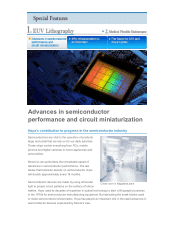
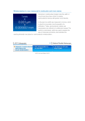
Advances in scaling down design rules (the width of
circuit lines) have been critical to making
semiconductor devices with greater circuit density.
In the past, line width was measured in microns, which
is short for micrometer (one thousandth of a
millimeter). Today, semiconductor makers use
nanometers (one millionth of a millimeter) instead. The
switch to nanometers, which are used to express the
size of molecules and atoms, demonstrates the
exacting demands now placed on semiconductor miniaturization.
Miniaturization is now measured in molecules and even atoms
HOYA Annual Re
p
ort 2011