Pentax 2011 Annual Report Download - page 10
Download and view the complete annual report
Please find page 10 of the 2011 Pentax annual report below. You can navigate through the pages in the report by either clicking on the pages listed below, or by using the keyword search tool below to find specific information within the annual report.-
 1
1 -
 2
2 -
 3
3 -
 4
4 -
 5
5 -
 6
6 -
 7
7 -
 8
8 -
 9
9 -
 10
10 -
 11
11 -
 12
12 -
 13
13 -
 14
14 -
 15
15 -
 16
16 -
 17
17 -
 18
18 -
 19
19 -
 20
20 -
 21
21 -
22
-
23
-
24
-
25
-
26
-
27
-
28
-
29
-
30
-
31
-
32
-
33
-
34
-
35
-
36
-
37
-
38
-
39
-
40
-
41
-
42
-
43
-
44
-
45
-
46
-
47
-
48
-
49
-
50
-
51
-
52
-
53
-
54
-
55
-
56
-
57
-
58
-
59
-
60
-
61
-
62
-
63
-
64
-
65
-
66
-
67
-
68
 |
 |
Many problems must be solved before manufacturers
can use EUV lithography on their production lines.
Interest in EUV first emerged more than 20 years ago.
The fact that this technology has not genuinely
reached the practical, mass productions stage shows
how high the technological barriers are.
Photomasks are instrumental to the transfer of circuit
patterns to silicon wafers. To make a photomask, the
pattern is placed on a glass substrate called a mask
blank. Unlike ArF lithography in which light is
transmitted through a transmission mask, EUV
lithography reflects light off of a defect-free reflection
mask to expose the circuit pattern. This is achieved
through light reflected by interlayer interference and
requires an ultra-multilayer membrane comprised of
several tens in alternating layers of molybdenum and
silicon. Each paired molybdenum-silicon layer is only
7.0nm thick, with a tolerance in precision of no more
than 0.01 nm. Precision membrane formation
technology is vital to achieving this level of accuracy. Moreover, the substrate’s flatness cannot
vary by more than 30nm. This is about four times more exacting than for conventional
photomask blanks. Furthermore, precision control is required for both sides of an EUV substrate.
Defects are not allowed: Imperfections on the blank will be transferred to the wafer. EUV
lithography uses light with a wavelength more than one order of magnitude smaller than with
conventional lithography. As a result, even imperfections with a height more than 20 times less
than the maximum permissible defect size for conventional lithography will become a phase shift
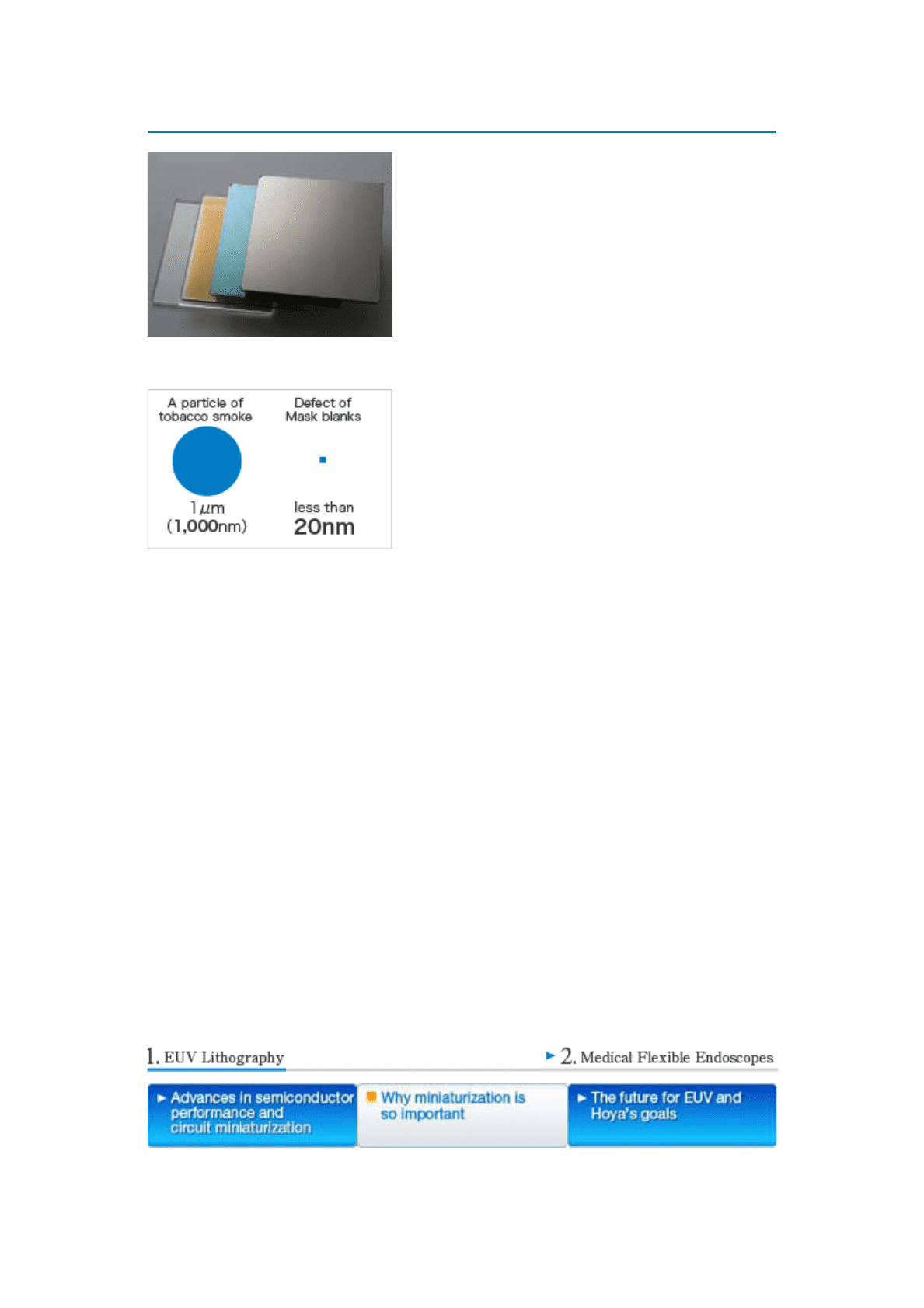
defect that is transferred to the wafer with EUV technology. This is why the blank can have no
defects larger than 30nm. As a frame of reference, a particle of tobacco smoke measures 1 μm
(micron) or smaller. This means a defect 1/30th the particulate size of tobacco smoke may not
be tolerable, which offers some idea of how microscopic and almost none-existent the defects
must be.
In relative terms, this would be the equivalent of not allowing a defect the size of single pollen on
a flat surface the size of a soccer field.
Until recently, it was this daunting nature of those many challenges that held progress in the
commercialization of EUV lithography back.
Taking on the challenging of achieving a breakthrough
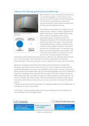
Mask blanks for semiconductor
production
HOYA Annual Re
p
ort 2011