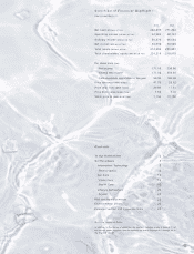
Pentax 2004 Annual Report Download - page 12
Download and view the complete annual report
Please find page 12 of the 2004 Pentax annual report below. You can navigate through the pages in the report by either clicking on the pages listed below, or by using the keyword search tool below to find specific information within the annual report.-
 1
1 -
 2
2 -
 3
3 -
 4
4 -
 5
5 -
 6
6 -
 7
7 -
 8
8 -
 9
9 -
 10
10 -
 11
11 -
 12
12 -
 13
13 -
 14
14 -
 15
15 -
 16
16 -
 17
17 -
 18
18 -
 19
19 -
 20
20 -
 21
21 -
 22
22 -
23
-
24
-
25
-
26
-
27
-
28
-
29
-
30
-
31
-
32
-
33
-
34
-
35
-
36
-
37
-
38
-
39
-
40
-
41
-
42
-
43
-
44
-
45
-
46
-
47
-
48
-
49
-
50
-
51
-
52
-
53
-
54
-
55
-
56
-
57
-
58
-
59
-
60
-
61
-
62
-
63
-
64
-
65
-
66
-
67
-
68
-
69
-
70
-
71
-
72
-
73
-
74
 |
 |

C
OMPETITIVENESS OF
H
OYA
’
SMASK BLANKS
10
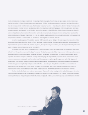
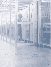
The principal factor underpinning the competitiveness of Hoya’s mask blanks is the rig-
orous quality management employed throughout the production process. Technicians at
the Nagasaka Plant in Yamanashi Prefecture use state-of-the-art equipment to achieve a
high level of technical expertise in polishing of the glass materials, and applying the
metallic film and resist coatings.
In the market for semiconductor mask blanks, demand was strong for phase shift mask blanks, in which Hoya’s high-
precision products hold a leading share, and sales increased. At the same time, the need for more precise technologies is
also increasing. Currently, the most common light source used in the steppers to expose circuit patterns onto silicon wafers
is krypton fluoride (KrF, wavelength 246nm*1), but it is becoming clear that as greater precision is required, argon fluoride
(ArF, wavelength 193nm) will be used for next-generation products.
In semiconductor photomasks, although Hoya’s market share is not large, the synergistic effect realized from
cutting-edge development assessment in mask blanks and LCD mask technologies is significant, making it an important
business for the Company. In terms of more high-precision products, Hoya has begun manufacturing masks following 90nm
design rules*2, and is currently working to implement mass production. Development has also been started on products
following 65nm design rules. Expansion of sales overseas was a priority issue during fiscal 2004, and Hoya’s products have
been highly praised by overseas customers.
Large-scale LCD photomasks are the master plates used in the manufacture of display panels found in LCD televi-
sions, PC monitors and mobile handset screens. Recovery in the PC market, shifting demand from CRT (Braun tube) to LCD
monitors, the increasing size of LCD monitors and expansion of the LCD television market all resulted in growing sales of
these photomasks.
Because Hoya’s production capacity was unable to keep pace with the rapid growth of the market, the Company is
pressing forward with the establishment of a production plant in Taiwan to add to its current facility in Kumamoto, Japan.
This new plant is scheduled to begin operating in the second half of fiscal 2004. A plant in Korea is also being planned as a
response to market expansion and optimization of production facilities. Large-scale masks for LCDs are becoming even
larger as LCD televisions increase in size and customers strengthen their cost competitiveness. Currently, the main sizes of
glass panels in production are the fifth*3and sixth*4generations. Certain manufacturers are planning to begin production
of the seventh*5generation in 2005, and are planning to build production lines for the eighth*6generation for some time
HOYA 2004-e 入稿用0705 04.7.22 7:59 PM ページ 11