Pentax 2012 Annual Report Download - page 9
Download and view the complete annual report
Please find page 9 of the 2012 Pentax annual report below. You can navigate through the pages in the report by either clicking on the pages listed below, or by using the keyword search tool below to find specific information within the annual report.-
 1
1 -
 2
2 -
 3
3 -
 4
4 -
 5
5 -
 6
6 -
 7
7 -
 8
8 -
 9
9 -
 10
10 -
 11
11 -
 12
12 -
 13
13 -
 14
14 -
 15
15 -
 16
16 -
 17
17 -
 18
18 -
 19
19 -
 20
20 -
21
-
22
-
23
-
24
-
25
-
26
-
27
-
28
-
29
-
30
-
31
-
32
-
33
-
34
-
35
-
36
-
37
-
38
-
39
-
40
-
41
-
42
-
43
-
44
-
45
-
46
-
47
-
48
-
49
-
50
-
51
-
52
-
53
-
54
-
55
-
56
-
57
-
58
-
59
-
60
-
61
-
62
-
63
-
64
-
65
-
66
-
67
-
68
-
69
-
70
-
71
-
72
-
73
-
74
-
75
-
76
 |
 |

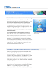
Mask blanks and photomasks are essential in the production of
semiconductor chips. They are the master plates used to transfer the minute,
highly complex circuit patterns for semiconductors onto the wafers that
become IC chips. A mask blank is a six-inch glass substrate polished
precisely* and coated with a metallic film and photosensitizing agent. This
substrate becomes a photomask when a circuit pattern is drawn onto it with
an electron beam (EB) or laser. In the production of semiconductors, an
exposure system is used to transfer the circuit pattern on the photomask onto
the semiconductor wafers.
* HOYA's mask blanks are polished flat to an accuracy of less than one thousandth of a
millimeter, with a surface roughness of only one millionth of a millimeter (one nanometer).
HOYA's mask blanks boast an overwhelming market share. The company
provides a wide variety of mask blanks, from those for leading-edge
development, to commoditized products, to semiconductor manufacturers
and photomask manufacturers in Japan and overseas. In addition to ensuring
a stable supply of high-quality products, HOYA customizes its products to suit
the process of each customer. It thus provides high added value, including
contributing to the improvement of customer yields.
Transfer image of circuit pattern in the
exposure process
As the circuit density of semiconductors has been growing greater, design
rules (the width of the lines of the circuit drawn on a wafer) have been
becoming finer every year — from 90nm to 65nm, 45nm, and 32nm. As of
2012, the line width of advanced circuits has been scaled down to as narrow
as 28nm, or even 22nm. Amid this trend toward miniaturization, fine circuit
patterns need to be drawn with high precision and resolution. The trend also
requires flawless quality, that is, mask blanks and photomasks with absolutely
no scratches or distortion.
Meanwhile, the development of extreme ultraviolet (EUV) lithography has
been in progress. EUV's wavelength is only 13.5nm, while the wavelength of
the ArF laser, the current light source of exposure systems used in
semiconductor production, is 193nm. As the next light source, EUV is being
Mask Blanks/Photomasks for Semiconductor Manufacturing
Toward Progress in the Miniaturization and Development of EUV Lithography