Pentax 2012 Annual Report Download - page 10
Download and view the complete annual report
Please find page 10 of the 2012 Pentax annual report below. You can navigate through the pages in the report by either clicking on the pages listed below, or by using the keyword search tool below to find specific information within the annual report.-
 1
1 -
 2
2 -
 3
3 -
 4
4 -
 5
5 -
 6
6 -
 7
7 -
 8
8 -
 9
9 -
 10
10 -
 11
11 -
 12
12 -
 13
13 -
 14
14 -
 15
15 -
 16
16 -
 17
17 -
 18
18 -
 19
19 -
 20
20 -
 21
21 -
22
-
23
-
24
-
25
-
26
-
27
-
28
-
29
-
30
-
31
-
32
-
33
-
34
-
35
-
36
-
37
-
38
-
39
-
40
-
41
-
42
-
43
-
44
-
45
-
46
-
47
-
48
-
49
-
50
-
51
-
52
-
53
-
54
-
55
-
56
-
57
-
58
-
59
-
60
-
61
-
62
-
63
-
64
-
65
-
66
-
67
-
68
-
69
-
70
-
71
-
72
-
73
-
74
-
75
-
76
 |
 |

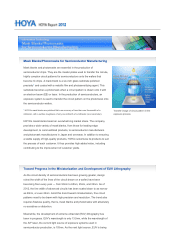
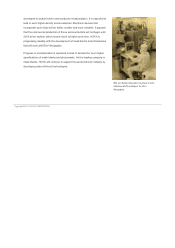
developed to enable further semiconductor miniaturization. It is expected to
lead to even higher-density semiconductors. Electronic devices that
incorporate such chips will be faster, smaller and more versatile. It appears
that the commercial production of these semiconductors will not begin until
2015 at the earliest, which means that it will take some time. HOYA is
progressing steadily with the development of mask blanks and photomasks
that will work with EUV lithography.
Progress in miniaturization is expected to lead to demand for even higher
specifications of mask blanks and photomasks. As the leading company in
mask blanks, HOYA will continue to support the semiconductor industry by
developing state-of-the-art technologies.
IBD (Ion Beam Deposition) system to form
reflective Mo/Si multilayer for EUV
lithography
Co
py
ri
g
ht 2012 © HOYA CORPORATION