Crucial 2014 Annual Report Download - page 9
Download and view the complete annual report
Please find page 9 of the 2014 Crucial annual report below. You can navigate through the pages in the report by either clicking on the pages listed below, or by using the keyword search tool below to find specific information within the annual report.-
 1
1 -
 2
2 -
 3
3 -
 4
4 -
 5
5 -
 6
6 -
 7
7 -
 8
8 -
 9
9 -
 10
10 -
 11
11 -
 12
12 -
 13
13 -
 14
14 -
 15
15 -
 16
16 -
 17
17 -
 18
18 -
 19
19 -
 20
20 -
21
-
22
-
23
-
24
-
25
-
26
-
27
-
28
-
29
-
30
-
31
-
32
-
33
-
34
-
35
-
36
-
37
-
38
-
39
-
40
-
41
-
42
-
43
-
44
-
45
-
46
-
47
-
48
-
49
-
50
-
51
-
52
-
53
-
54
-
55
-
56
-
57
-
58
-
59
-
60
-
61
-
62
-
63
-
64
-
65
-
66
-
67
-
68
-
69
-
70
-
71
-
72
-
73
-
74
-
75
-
76
-
77
-
78
-
79
-
80
-
81
-
82
-
83
-
84
-
85
-
86
-
87
-
88
-
89
-
90
-
91
-
92
-
93
-
94
-
95
-
96
-
97
-
98
-
99
-
100
-
101
-
102
-
103
-
104
-
105
-
106
-
107
-
108
-
109
-
110
-
111
-
112
-
113
-
114
-
115
-
116
-
117
-
118
-
119
-
120
-
121
-
122
-
123
-
124
-
125
-
126
-
127
-
128
-
129
-
130
-
131
-
132
-
133
-
134
-
135
-
136
-
137
-
138
-
139
-
140
-
141
-
142
-
143
-
144
-
145
-
146
-
147
-
148
-
149
-
150
-
151
-
152
-
153
-
154
-
155
-
156
-
157
 |
 |
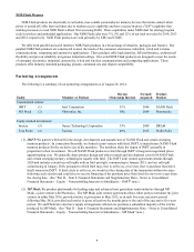
7
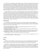
Product Warranty
Because the design and manufacturing process for semiconductor products is highly complex, it is possible that we may
produce products that do not comply with customer specifications, contain defects or are otherwise incompatible with end
uses. In accordance with industry practice, we generally provide a limited warranty that our products are in compliance with
our specifications existing at the time of delivery. Under our general terms and conditions of sale, liability for certain failures
of product during a stated warranty period is usually limited to repair or replacement of defective items or return of, or a credit
with respect to, amounts paid for such items. Under certain circumstances, we provide more extensive limited warranty
coverage than that provided under our general terms and conditions.
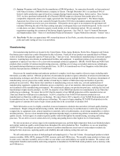
Competition
We face intense competition in the semiconductor memory market from a number of companies, including Samsung
Electronics Co., Ltd.; SanDisk Corporation; SK Hynix Inc. and Toshiba Corporation. Some of our competitors are large
corporations or conglomerates that may have greater resources to withstand downturns in the semiconductor markets in which
we compete, invest in technology and capitalize on growth opportunities. Our competitors seek to increase silicon capacity,
improve yields, reduce die size and minimize mask levels in their product designs resulting in significantly increased
worldwide supply and downward pressure on prices. Many of our high-volume memory products are manufactured to industry
standard specifications and as such have similar performance characteristics to those of our competitors. For these high-
volume memory products, the principal competitive factors are generally price and performance characteristics including:
operating speed, power consumption, reliability, compatibility, size and form factors. For our other memory products, the
aforementioned performance characteristics generally take precedence to pricing.
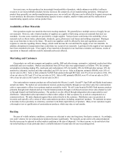
Research and Development
Our process technology R&D efforts are focused primarily on development of successively smaller line-width process
technologies, as well as new, fundamentally different memory structures, materials and packages, which are designed to
facilitate our transition to next generation memory products. Additional process technology R&D efforts focus on the
enablement of advanced computing and mobile memory architectures, the investigation of new opportunities that leverage our
core semiconductor expertise and the development of new manufacturing materials. Product design and development efforts
include our high density DDR3 and DDR4 DRAM and LPDRAM products as well as high density and mobile NAND Flash
memory (including 3D NAND and MLC and TLC technologies), NOR Flash memory, specialty memory, SSDs, HMCs and
other memory technologies and systems.
Our R&D expenses were $1.37 billion, $931 million and $918 million in 2014, 2013 and 2012, respectively. We share
certain R&D process technology and design costs for NAND Flash and emerging technologies with Intel. We shared R&D
process and design costs for DRAM with Nanya through December 2012, when our cost-sharing agreement was terminated.
As a result of reimbursements under our Intel and Nanya cost-sharing arrangements, our overall R&D expenses were reduced
by $137 million, $146 million and $225 million in 2014, 2013 and 2012, respectively.
To compete in the semiconductor memory industry, we must continue to develop technologically advanced products and
processes. We believe that expansion of our semiconductor product offerings is necessary to meet expected market demand for
specific memory solutions. Our process, design and package development efforts occur at multiple locations across the world,
with our largest R&D centers located in Boise, Idaho; Hiroshima, Japan; Hashimoto, Japan; and Milpitas, California. We have
several additional product design centers in other strategic locations around the world. In addition, we develop
photolithography mask technology at our MP Mask joint venture facility in Boise.
R&D expenses vary primarily with the number of development wafers processed, the cost of advanced equipment
dedicated to new product and process development and personnel costs. Because of the lead times necessary to manufacture
our products, we typically begin to process wafers before completion of performance and reliability testing. We deem
development of a product complete once the product has been thoroughly reviewed and tested for performance and reliability.
R&D expenses can vary significantly depending on the timing of product qualification.