Nikon 2004 Annual Report Download - page 17
Download and view the complete annual report
Please find page 17 of the 2004 Nikon annual report below. You can navigate through the pages in the report by either clicking on the pages listed below, or by using the keyword search tool below to find specific information within the annual report.-
 1
1 -
2
-
3
-
4
-
5
-
6
-
 7
7 -
 8
8 -
 9
9 -
 10
10 -
 11
11 -
 12
12 -
 13
13 -
 14
14 -
 15
15 -
 16
16 -
 17
17 -
 18
18 -
 19
19 -
 20
20 -
 21
21 -
 22
22 -
 23
23 -
 24
24 -
 25
25 -
 26
26 -
 27
27 -
28
-
29
-
30
-
31
-
32
-
33
-
34
-
35
-
36
-
37
-
38
-
39
-
40
-
41
-
42
-
43
-
44
-
45
-
46
 |
 |

researchanddevelopment
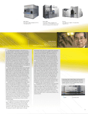
1. Nailembeddedinacookie
2. Terahertzimagemakesitpos-
sibletoseethenailinsidethe
cookie
3. Terahertzimage(enlarged)
Terahertz(THz)technology
Terahertzlightisarelativelyunusedpartofthe
electromagneticwavethatofferssignificantpotential
advantagesoverX-raysforlookinginsideawidevari-
etyofobjects.Withafrequencyrangearound1012Hz
(1THz,oronetrillionhertz)betweenvisiblelightand
radiowaves,terahertzlightpassesthroughnon-me-
tallicsubstancessuchaspaperandrubber.Detectors
builtusingterahertzlightcouldthusprovideawide
rangeofsecuritybenefits,suchasnon-invasivescreen-
ingofmailforbannedsubstancesorexplosives,for
example.Otherpotentialapplicationsincludemedical
scansforcancercellsortumorsandfoodtestingto
detectdangeroussubstances.
TochigiNikonCorporationisthefirstcompanyin
theworldtodevelopacommercialproductbasedon
terahertztechnology.Theterahertzpulsespectrome-
terisabletorecognizesubstancesusingterahertzlight
shinedontotheobjectpassesthroughorisreflected.
SincethesystemdebutedinFebruary2004,several
machineshavealreadybeensoldtoresearchinstitu-
tionsinJapan.
TochigiNikonisalsodevelopingreal-timeTHz
imagingsystems.Thistechnologyhasthepotentialto
providesaferbodyscanningcapabilitiesthanX-rays.It
promisestoyieldsignificantadvancesinfieldssuchas
securityandmedicine.
Nikon’sresearchanddevelopmentactivitiesfocuson
opto-electronicsandprecisiontechnologies,areas
whereNikonhashoneditscompetitiveedgeover
decades.Bycombiningcoretechnicalexpertisewith
digital,control,informationandcommunications
technologies,NikonR&Dteamsareinvolvedinthe
developmentofmanyinnovativeproductsthatbring
togetherthebenefitsofdifferentavenuesofscientific
research.
ThenucleusoftechnicaldevelopmentatNikonis
theCoreTechnologyCenter,whichundertakesbasic
researchfromalong-termperspectiveandisalso
engagedinthedevelopmentofcutting-edgetechnol-
ogy.Thein-housecompaniesandNikonGroupfirms
alsoconductvariousR&Dprograms.
Thisreportspotlightstwoareaswithunique
potential:MEMSandterahertztechnologies.
MicroElectroMechanicalSystem(MEMS)
technology
MEMStechnologyinvolveselectromechanicalsystems
thatoperateatthemicroscopiclevel.Nikonhas
developedanumberofsuchdevicesusingitscore
technicalexpertiseinvariousareas.Oneexampleis
aself-assemblingmicroarrayofmirrors.Nikonhas
succeededincreatingimpressivelysolidstructures
fromthinfilmsofthesemirrors,despitethefilms
havingathicknessoflessthanonemicrometer.The
internalstresscharacteristicsofthethin-filmstructure
resultinthespontaneouscreationofthin-film
mirrorsofapproximately50micrometersquarein
area(picturedtopleft).Thesemirrorsassembleinto
anintegratedwhole,ontowhichisaddedanarray
ofmicroactuatorsthatcanmovevertically(pictured
topright).ThewholecreatesaMEMSstructurethat
combinesanumberofNikontechnologies.
MEMStechnologybringstogethermanyofNikon’s
proprietaryskillsinspatialoptics,includinglenses,
prismsandmirrors.Itheraldstheadventofnewopti-
caldevicesandawiderangeoffascinatingtechnical
possibilitiesthathithertocouldonlybeimagined.
M E M S
1
2
3
15