Fujitsu 2001 Annual Report Download - page 17
Download and view the complete annual report
Please find page 17 of the 2001 Fujitsu annual report below. You can navigate through the pages in the report by either clicking on the pages listed below, or by using the keyword search tool below to find specific information within the annual report.-
 1
1 -
2
-
3
-
4
-
5
-
6
-
 7
7 -
 8
8 -
 9
9 -
 10
10 -
 11
11 -
 12
12 -
 13
13 -
 14
14 -
 15
15 -
 16
16 -
 17
17 -
 18
18 -
 19
19 -
 20
20 -
 21
21 -
 22
22 -
 23
23 -
 24
24 -
 25
25 -
 26
26 -
 27
27 -
28
-
29
-
30
-
31
-
32
-
33
-
34
-
35
-
36
-
37
-
38
-
39
-
40
-
41
-
42
-
43
-
44
-
45
-
46
-
47
-
48
-
49
-
50
-
51
-
52
 |
 |

15
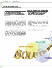
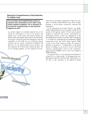
Assembly of optical devices
Electronic Devices
Pursuing strong earnings through
rigorous selection and concentration
*FCRAM: Fast Cycle Random Access Memory
FRAM: Ferroelectric Random Access Memory
FRAM is a registered trademark of U.S.-based Ramtron International Corporation.
SAW: Surface Acoustic Wave
In our electronic devices business, our basic objective is to
secure a foundation for strong earnings through rigorous
selection and concentration on high-growth markets,
pursuing a strategy of becoming leaders in those markets.
Positioning ourselves to capitalize on the anticipated
growth markets of the broadband Internet era and grow our
business in devices for such areas as mobile terminals,
digital appliances and networks, we are concentrating on
system LSI chips and flash memory, as well as high
value–added products like compound semiconductors,
FCRAM, FRAM and SAW devices.
In regard to capital expenditures, preserving a healthy
cash flow is our main concern. We give priority to investing
in key products, and we are increasing the efficiency of our
capital expenditures by strict targeting of our investments,
making better use of our cooperative ventures and foundry
partners, and exploiting the full potential of our existing
facilities. Our cooperative ventures include a flash memory
joint venture with Advanced Micro Devices (AMD),
cooperation with Sony to develop and produce chips
integrating logic with embedded DRAM, and a project to
develop next-generation FCRAM technology in cooperation
with Toshiba and Winbond Electronics in Taiwan. These
are just some of the ways in which we are trying to speed
up our development processes and enhance the
competitiveness of our products.
Regarding product-specific strategies, for system LSI,
we are working to enhance earnings by concentrating our
resources in fields with high growth potential, such as
digital AV, mobile communications, and WAN/high-end
LAN. In flash memory, we are developing a wide range of
new markets beyond cellular telephones, including
communication networks and digital AV appliances. The
Fujitsu Group holds the leading market position in Japan
for flash memory and is also among the global leaders in
this category, an achievement which stems from our
technological edge in areas such as compact packaging and
superior production capabilities. In compound
semiconductors, we are focusing our efforts on the market
for high-speed, high-capacity optical transmission
systems—an area poised for expansion with the spread of
broadband Internet. In FCRAMs, we are taking full
advantage of this technology’s high speed and low power
consumption to develop and offer new products for the
cellular phone and network markets ahead of our
competition. In the area of FRAM, we are expanding our
sales to the IC-card and smart-card markets—areas which
are expected to grow with the development of e-commerce
and mobile networks—and are promoting our products as
de facto standards in these markets. In SAW devices, by
maintaining the top share in the mobile communications
market, we are aiming to secure a foundation for strong
earnings going forward.
With regard to development and production facilities,
we opened the Fujitsu Akiruno Technology Center in July
2000 to serve as our base for developing electronic devices.
This facility combines our process development and
research divisions, and will soon have prototype production
lines, as well, enabling us to accelerate the development of
process technologies. Also in July 2000, Fujitsu AMD
Semiconductor Limited began construction of a third flash
memory plant in Aizu-Wakamatsu with production to begin
in August 2001. In plasma display panels (PDPs), Fujitsu-
Hitachi Plasma Display Limited completed construction of
the world’s largest mass production plant for PDPs and
began product shipments in April 2001. The new plant is
producing 32-inch and 37-inch PDPs for household use, in
addition to 42-inch models.