Nikon 2008 Annual Report Download - page 12
Download and view the complete annual report
Please find page 12 of the 2008 Nikon annual report below. You can navigate through the pages in the report by either clicking on the pages listed below, or by using the keyword search tool below to find specific information within the annual report.-
 1
1 -
 2
2 -
 3
3 -
 4
4 -
 5
5 -
 6
6 -
 7
7 -
 8
8 -
 9
9 -
 10
10 -
 11
11 -
 12
12 -
 13
13 -
 14
14 -
 15
15 -
 16
16 -
 17
17 -
 18
18 -
 19
19 -
 20
20 -
 21
21 -
 22
22 -
23
-
24
-
25
-
26
-
27
-
28
-
29
-
30
-
31
-
32
-
33
-
34
-
35
-
36
-
37
-
38
-
39
-
40
-
41
-
42
-
43
-
44
-
45
-
46
-
47
-
48
-
49
-
50
-
51
-
52
-
53
-
54
-
55
-
56
-
57
-
58
 |
 |

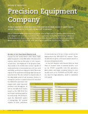
KAZUO USHIDA
Director, Member of the Board &
Senior Executive Officer
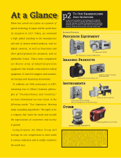
President of Precision Equipment Company
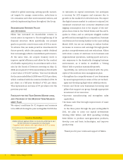
Securing the leading market share for high-
end models will also lessen the risk of the silicon
investment cycle, the market fluctuations peculiar
to the semiconductor industry. It will provide a
further benefit in terms of the cutbacks in capital
expenditures by semiconductor makers, since the
trend toward investment in cutting-edge models is
likely to continue as manufacturers place priority
on investment in device shrinkage to produce high-
value-added semiconductors.
Multi-Lens Projection Optical System
Allows LCD Scanners to Adapt to the
10th Generation
The key to the market for LCD steppers and scan-
ners is for the most part the trend toward larger
LCD televisions. Manufacturing of panels 50 inches
or larger will be more efficient using 10th genera-
tion large glass plates. As LCD panels become larger,
Nikon is able to develop and manufacture equip-
ment that easily adapts to the larger glass plates by
using a multi-lens projection optical system. This
system has allowed Nikon to capture a substan-
tial share of the market for lithography equipment
compatible with 7th and 8th generation plates. This
competitive advantage will not change with the
progress to the next generation.
Launch Planned for Products for the
New Double Patterning Technique
Double patterning is a technique to enhance reso-
lution by dividing the exposure into two separate
processes, and is increasingly looked to as the
technology for mass production of semiconduc-
tors at 30 nm level node. The exposure requires a
higher alignment accuracy than with conventional
techniques. Improvement in the throughput is
also essential to maintain productivity with the
double exposure.
Nikon is currently developing an ArF immersion
scanner for double patterning, the improved NSR-
S610C model, with significantly enhanced align-
ment accuracy and faster stage operating speed to
raise throughput. We plan to bring this new model
to market in the year ending March 2009.
As we develop this new technology we are also
looking to further reduce costs by utilizing a sim-
plified design to minimize manufacturing time and
effort by reviewing the production process, and
have adopted a platform in which the modules are
shared among models as much as possible.
10 Nikon Annual Report 2008