Nikon 2009 Annual Report Download - page 11
Download and view the complete annual report
Please find page 11 of the 2009 Nikon annual report below. You can navigate through the pages in the report by either clicking on the pages listed below, or by using the keyword search tool below to find specific information within the annual report.-
 1
1 -
 2
2 -
 3
3 -
 4
4 -
 5
5 -
 6
6 -
 7
7 -
 8
8 -
 9
9 -
 10
10 -
 11
11 -
 12
12 -
 13
13 -
 14
14 -
 15
15 -
 16
16 -
 17
17 -
 18
18 -
 19
19 -
 20
20 -
 21
21 -
 22
22 -
23
-
24
-
25
-
26
-
27
-
28
-
29
-
30
-
31
-
32
-
33
-
34
-
35
-
36
-
37
-
38
-
39
-
40
-
41
-
42
-
43
-
44
-
45
-
46
-
47
-
48
-
49
-
50
-
51
-
52
-
53
-
54
-
55
-
56
-
57
-
58
-
59
-
60
 |
 |

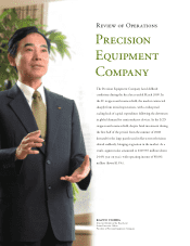
Review of the Year Ended March 2009
In the IC steppers and scanners field, Nikon took steps to
expand sales of cutting-edge equipment such as the NSR-
S610C ArF immersion scanner (the world’s first scanner
capable of mass production of semiconductors at 45 nm
applications and beyond), and marketed EUV lithography
equipment (extreme ultraviolet system for research and
development) that enables further device shrinkage.
In the LCD steppers and scanners field, Nikon worked
to expand sales of the existing FX-65S model for litho-
graphic exposure of 6th generation glass plates, as well
as the FX-903N model, which is ideally suited for the
manufacture of the small to medium-sized high-precision
liquid crystal displays used in cell phones and automotive
electronic devices. In addition, we initiated shipments of
FX-101S lithography equipment, which is compatible with
10th generation glass plates.
We also continued our concerted efforts throughout the
Precision Equipment Company to boost cost-competitive-
ness by shortening manufacturing periods, as well as
adopting simplified designs and common platforms.
NSR-S620 ArF Immersion Scanner to Be Introduced
in the Year Ending March 2010
Despite the difficult business environment for IC steppers
and scanners, for the year ending March 2010 Nikon is
focusing on double patterning,*1 one of the most promis-
ing next-generation lithography techniques. Specifically,
we are developing an ArF immersion scanner for double
patterning that will allow for 32 nm device production.
For successful development, two issues must be resolved.
The first is improvement in alignment accuracy. Since
double patterning involves the overlaying of two layers to
create the pattern, alignment requires extreme precision.
Currently, the alignment accuracy requirement is around
7 nm, but double patterning will require a reduction to
half or even one-third of that figure.
The second issue is enhancing throughput (the number
of wafers exposed in a given period). Since double pat-
terning consists of two exposures, the throughput must be
doubled to maintain the current level of productivity in
the customer’s manufacturing process.
The NSR-S620 ArF immersion scanner for mass pro-
duction with double patterning that Nikon will introduce
utilizes new concepts which will provide the necessary
precision and throughput. This system will be extremely
competitive not only in terms of precision alignment but
also in offering an exceptional throughput level, an aspect
in which our rival has been considered superior. We plan
to begin shipments in the third quarter of the year end-
ing March 2010 (October to December 2009). We have
adopted a new design concept for the NSR-S620 in which
the overall system is created from 13 individual modules,
allowing for a considerably shorter period from shipment
to operation at the customer’s site.
Currently Nikon is constructing a new building at the
Kumagaya Plant with a highly efficient clean room that
will be used to produce the NSR-S620 and enhance its
competitiveness. With the focus of effort on the NSR-
S620, Nikon seeks to quickly gain a leading share of the
market for high-end IC steppers and scanners.
Note:
1. Double patterning is a lithography technique in which a single, dense circuit
pattern is split into two coarser patterns that can be exposed separately. The two
patterns can then be overlaid on the wafer, providing a final, dense circuit pattern.
MARKET ENVIRONMENT AND BUSINESS TRENDS
Business conditions for the semiconductor-related industry will likely remain difficult, with device manufacturers showing
continued caution regarding capital expenditures. The LCD panel market is also expected to lack transparency, despite some
signs of rising operation rates among panel manufacturers.
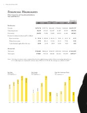
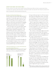
219,915
290,814
291,913
200920082007
Net Sales
(Millions of yen)
Years ended March 31
Operating Income
(Millions of yen)
Years ended March 31
8,041
43,348
49,321
200920082007
Nikon Annual Report 2009 9