Nikon 2005 Annual Report Download - page 11
Download and view the complete annual report
Please find page 11 of the 2005 Nikon annual report below. You can navigate through the pages in the report by either clicking on the pages listed below, or by using the keyword search tool below to find specific information within the annual report.-
 1
1 -
 2
2 -
 3
3 -
 4
4 -
 5
5 -
 6
6 -
 7
7 -
 8
8 -
 9
9 -
 10
10 -
 11
11 -
 12
12 -
 13
13 -
 14
14 -
 15
15 -
 16
16 -
 17
17 -
 18
18 -
 19
19 -
 20
20 -
 21
21 -
 22
22 -
23
-
24
-
25
-
26
-
27
-
28
-
29
-
30
-
31
-
32
-
33
-
34
-
35
-
36
-
37
-
38
-
39
-
40
-
41
-
42
-
43
-
44
-
45
-
46
-
47
-
48
-
49
-
50
 |
 |

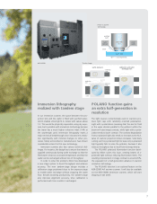
High throughput, improved alignment accuracy and the
incorporation of an ultra-high N.A. projection lens enable the
mass production of next-generation 110nm devices with this
lens scanning KrF excimer stepper.
NSR-S208D
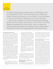
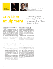
LCD exposure system business performing
well as panel sizes increase
The LCD exposure system business posted excel-
lent results in the year ended March 2005. Nikon
has developed an original multi-lens scanning
system for use in LCD exposure systems that is
ideally suited to larger substrates. This applica-
tion of parallel multi-lens units promises to result
in greater benefi ts for LCD manufacturers as
panel sizes continue to increase. In June 2005,
Nikon began shipment of the latest LCD exposure
systems for 7th and 8th generation production
processes (FX-71S).
Reductions achieved in stepper lead times
and costs
A major factor in the turnaround in profi tability
of Nikon’s precision equipment operations has
been a steep reduction in scanner production
lead times. For leading-edge IC scanners, it now
takes about six months from lens fabrication to
fi nal installation, which is roughly half the previ-
ous fi gure. Simplifi ed design has played a part
in this achievement, covering all processes from
development and design to technical and manu-
facturing steps. Nikon teams have also worked
with external contractors to reduce lead times
and achieve demanding performance targets.
The benefi ts of simplifi ed design are only just
becoming apparent, and Nikon expects the new
processes to generate further productivity gains
going forward. Nikon has also thoroughly revised
the sequence within manufacturing to eliminate
any waste created by repeated processes. On
the product side, Nikon has sought to improve
the quality of the fi nished form in production
to eliminate any interference between modules,
thereby reducing assembly time. The reductions
in lead times achieved to date have also gener-
ated substantial cost reductions.
FX-81S
This large-plate exposure system supports eighth-
generation plate sizes for LCDs, with improved
throughput and a multi-lens projection optical
system for greater productivity.
NSR-SF140
Providing superior cost performance, high resolution and
throughput, this i-line scan fi eld stepper is optimized for mix-
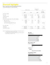
and-match solutions. 11, 3 87
(20,806)
(24,595)
05
04
03
Operating Income (Loss)
(millions of yen)
Net Sales*
(millions of yen)
214,326
158,054
133,102
05
04
03
CY 01 02 03 04 05 06 07 08 09 10 11 12 13 14 15 16
Technology Node hp130 hp90 hp65 hp45 hp32 hp22
DRAM Half Pitch130 115 10 0 90 807065 57 50 45 40 35 32 2825 22
MPU Gate in resist 90 65 53 45 40 35 32 2825 22 20 1817 15 13
post-etch65 45 37 32 2825 22 20 1816 14 13 11 10 9
Nikon Lithography Roadmap
*The above fi gures include intersegment sales.
Critical layer
exposure
method
KrF
248nm
ArF EUV
13nm
193nm
dry immersion
(water)
EPL 100keV
ITRS 2004
9